JAJSQE3 may 2023 SN74LV2T74
PRODUCTION DATA
- 1
- 1 特長
- 2 アプリケーション
- 3 概要
- 4 Revision History
- 5 Pin Configuration and Functions
-
6 Specifications
- 6.1 Absolute Maximum Ratings
- 6.2 ESD Ratings
- 6.3 Recommended Operating Conditions
- 6.4 Thermal Information
- 6.5 Electrical Characteristics
- 6.6 Timing Characteristics 1.8-V VCC
- 6.7 Timing Characteristics 2.5-V VCC
- 6.8 Timing Characteristics 3.3-V VCC
- 6.9 Timing Characteristics 5-V VCC
- 6.10 Switching Characteristics 1.8-V VCC
- 6.11 Switching Characteristics 2.5-V VCC
- 6.12 Switching Characteristics 3.3-V VCC
- 6.13 Switching Characteristics 5-V VCC
- 6.14 Noise Characteristics
- 6.15 Typical Characteristics
- 7 Parameter Measurement Information
- 8 Detailed Description
- 9 Application and Implementation
- 10Power Supply Recommendations
- 11Device and Documentation Support
- 12Mechanical, Packaging, and Orderable Information
パッケージ・オプション
メカニカル・データ(パッケージ|ピン)
サーマルパッド・メカニカル・データ
- BQA|14
発注情報
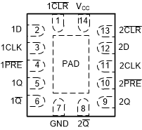
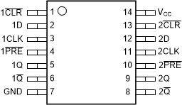
5 Pin Configuration and Functions
 Figure 5-1 BQA Package, 14-Pin WQFN
(Top View)
 Figure 5-2 PW Package, 14-Pin TSSOP
(Top View)
Figure 5-2 PW Package, 14-Pin TSSOP
(Top View)Table 5-1 Pin Functions
| PIN | TYPE | DESCRIPTION | |
|---|---|---|---|
| NAME | NO. | ||
| 1CLR | 1 | Input | Clear for channel 1, active low |
| 1D | 2 | Input | Data for channel 1 |
| 1CLK | 3 | Input | Clock for channel 1, rising edge triggered |
| 1PRE | 4 | Input | Preset for channel 1, active low |
| 1Q | 5 | Output | Output for channel 1 |
| 1Q | 6 | Output | Inverted output for channel 1 |
| GND | 7 | — | Ground |
| 2Q | 8 | Output | Inverted output for channel 2 |
| 2Q | 9 | Output | Output for channel 2 |
| 2PRE | 10 | Input | Preset for channel 2, active low |
| 2CLK | 11 | Input | Clock for channel 2, rising edge triggered |
| 2D | 12 | Input | Data for channel 2 |
| 2CLR | 13 | Input | Clear for channel 2, active low |
| VCC | 14 | — | Positive supply |
| Thermal Pad(1) | — | The thermal pad can be connected to GND or left floating. Do not connect to any other signal or supply | |
(1) BQA package only.