SCLS469F March 2003 – December 2014 SN74LV4052A-Q1
PRODUCTION DATA.
- 1 Features
- 2 Applications
- 3 Description
- 4 Revision History
- 5 Pin Configuration and Functions
- 6 Specifications
- 7 Parameter Measurement Information
- 8 Detailed Description
- 9 Application and Implementation
- 10Power Supply Recommendations
- 11Layout
- 12Device and Documentation Support
- 13Mechanical, Packaging, and Orderable Information
パッケージ・オプション
メカニカル・データ(パッケージ|ピン)
サーマルパッド・メカニカル・データ
- D|16
発注情報
9 Application and Implementation
NOTE
Information in the following applications sections is not part of the TI component specification, and TI does not warrant its accuracy or completeness. TI’s customers are responsible for determining suitability of components for their purposes. Customers should validate and test their design implementation to confirm system functionality.
9.1 Application Information
A multiplexer is used in applications where multiple signals share a resource. In the example below, several different sensors are connected to the analog-to-digital converter (ADC) of a microcontroller (MCU).
9.2 Typical Application
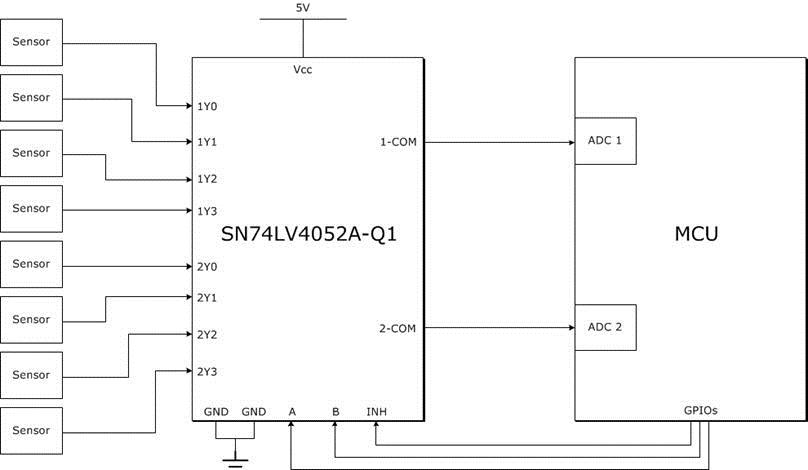 Figure 11. Typical Application Schematic
9.2.1 Design Requirements
Normally processing 8 different analog signals would require 8 separate ADCs, but this figure shows how to achieve this using only 2 ADCs and 3 GPIOs (general purpose input/outputs).
9.2.2 Detailed Design Procedure
To design with the SN74LV4052A-Q1, a stable input voltage between 2V (seeRecommended Operating Conditions for details) and 5.5 V must be available. Another important design consideration would be the characteristics of the signal that is being multiplexed to make sure no important information is lost due to timing or voltage level incompatibility with this device.