SCAS291W MARCH 1993 – October 2016 SN54LVC138A , SN74LVC138A
PRODUCTION DATA.
- 1 Features
- 2 Applications
- 3 Description
- 4 Revision History
- 5 Pin Configuration and Functions
- 6 Specifications
- 7 Parameter Measurement Information
- 8 Detailed Description
- 9 Application and Implementation
- 10Power Supply Recommendations
- 11Layout
- 12Device and Documentation Support
- 13Mechanical, Packaging, and Orderable Information
パッケージ・オプション
デバイスごとのパッケージ図は、PDF版データシートをご参照ください。
メカニカル・データ(パッケージ|ピン)
- DB|16
- PW|16
- NS|16
- RGY|16
- D|16
- DGV|16
- RSV|16
サーマルパッド・メカニカル・データ
- RGY|16
発注情報
11 Layout
11.1 Layout Guidelines
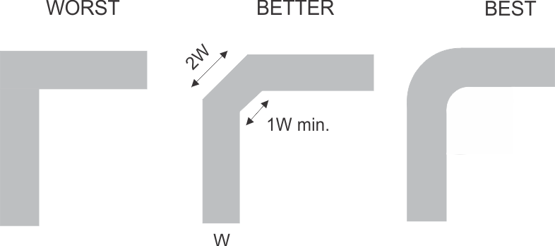
Reflections and matching are closely related to loop antenna theory, but different enough to warrant their own discussion. When a PCB trace turns a corner at a 90° angle, a reflection can occur. This is primarily due to the change of width of the trace. At the apex of the turn, the trace width is increased to 1.414 times its width. This upsets the transmission line characteristics, especially the distributed capacitance and self–inductance of the trace (resulting in the reflection). It is a given that not all PCB traces can be straight, and so they have to turn corners. Figure 5 shows progressively better techniques of rounding corners. Only the last example maintains constant trace width and minimizes reflections.
11.2 Layout Example
 Figure 5. Trace Example