SCES414P November 2002 – November 2016 SN74LVC1G57
PRODUCTION DATA.
- 1 Features
- 2 Applications
- 3 Description
- 4 Revision History
- 5 Pin Configuration and Functions
- 6 Specifications
- 7 Parameter Measurement Information
- 8 Detailed Description
- 9 Application and Implementation
- 10Power Supply Recommendations
- 11Layout
- 12Device and Documentation Support
- 13Mechanical, Packaging, and Orderable Information
パッケージ・オプション
メカニカル・データ(パッケージ|ピン)
サーマルパッド・メカニカル・データ
- DRY|6
発注情報
8 Detailed Description
8.1 Overview
The SN74LVC1G57 device features configurable multiple functions. The output state is determined by eight patterns of 3-bit input. The user can choose the logic functions AND, OR, NAND, NOR, XNOR, inverter, and buffer. All inputs can be connected to VCC or GND.
The CMOS device has high output drive while maintaining low static power dissipation over a broad VCC operating range.
This configurable multiple-function gate is designed for 1.65-V to 5.5-V VCC operation.
8.2 Functional Block Diagram

8.3 Feature Description
8.3.1 Schmitt-Trigger Inputs
Schmitt-trigger inputs are designed to provide a minimum separation between positive and negative switching thresholds. This allows for noisy or slow inputs that would cause problems such as oscillation or excessive current draw with normal CMOS inputs
8.3.2 Inputs Accept Voltages to 5.5 V
The SN74LVC1G57 is a configurable multiple-function gate is designed for 1.65-V to 5.5-V VCC operation. Inputs are over-voltage tolerant up to 5.5 V. This feature allows the use of this device as a translator in a mixed 1.8-V, 3.3-V, and 5-V system environment.
8.4 Device Functional Modes
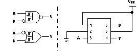
Table 1 lists the functional modes of the SN74LVC1G57 and Table 2 lists the logic configuration images.
Table 1. Function Table
| INPUTS | OUTPUT | ||
|---|---|---|---|
| In2 | In1 | In0 | Y |
| L | L | L | H |
| L | L | H | L |
| L | H | L | H |
| L | H | H | L |
| H | L | L | L |
| H | L | H | L |
| H | H | L | H |
| H | H | H | H |
Table 2. Logic Configurations
| LOGIC FUNCTION | FIGURE NO. |
|---|---|
| 2-Input AND | Figure 4 |
| 2-Input AND with both inputs inverted | Figure 7 |
| 2-Input NAND with inverted input | Figure 5 and Figure 6 |
| 2-Input OR with inverted input | Figure 5 and Figure 6 |
| 2-Input NOR | Figure 7 |
| 2-Input NOR with both inputs inverted | Figure 4 |
| 2-Input XNOR | Figure 8 |
 Figure 4. 2-Input AND Gate
 Figure 6. 2-Input NAND Gate With Inverted B Input
 Figure 5. 2-Input NAND Gate With Inverted A Input
 Figure 7. 2-Input NOR Gate
 Figure 8. 2-Input XNOR Gate