JAJSD24 March   2017 SN74LVC1G86-Q1

PRODUCTION DATA.  

  1. 特長
  2. アプリケーション
  3. 概要
  4. 改訂履歴
  5. Pin Configuration and Functions
  6. Specifications
    1. 6.1 Absolute Maximum Ratings
    2. 6.2 ESD Ratings
    3. 6.3 Recommended Operating Conditions
    4. 6.4 Thermal Information
    5. 6.5 Electrical Characteristics
    6. 6.6 Switching Characteristics, CL = 30 pF or 50 pF
    7. 6.7 Operating Characteristics
    8. 6.8 Typical Characteristics
  7. Parameter Measurement Information
  8. Detailed Description
    1. 8.1 Overview
    2. 8.2 Functional Block Diagram
    3. 8.3 Feature Description
      1. 8.3.1 Balanced High-Drive CMOS Push-Pull Outputs
      2. 8.3.2 Standard CMOS Inputs
      3. 8.3.3 Clamp Diodes
      4. 8.3.4 Partial Power Down (Ioff)
      5. 8.3.5 Over-voltage Tolerant Inputs
    4. 8.4 Function Table
  9. Application and Implementation
    1. 9.1 Application Information
    2. 9.2 Typical Application
      1. 9.2.1 Design Requirements
      2. 9.2.2 Detailed Design Procedure
      3. 9.2.3 Application Curve
  10. 10Power Supply Recommendations
  11. 11Layout
    1. 11.1 Layout Guidelines
    2. 11.2 Layout Example
  12. 12デバイスおよびドキュメントのサポート
    1. 12.1 ドキュメントの更新通知を受け取る方法
    2. 12.2 コミュニティ・リソース
    3. 12.3 商標
    4. 12.4 静電気放電に関する注意事項
    5. 12.5 Glossary
  13. 13メカニカル、パッケージ、および注文情報

パッケージ・オプション

メカニカル・データ(パッケージ|ピン)
サーマルパッド・メカニカル・データ
発注情報

Pin Configuration and Functions

DCK Package
5-Pin SC70
Top View
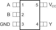
SN74LVC1G86-Q1 po1_DCK_ces222.gif

Pin Functions(1)

PIN I/O DESCRIPTION
NO. NAME
1 A I Input A
2 B I Input B
3 GND Ground
4 Y O Output Y
5 VCC Positive Supply
See mechanical drawings for dimensions.