JAJSTR0A March 2024 – May 2024 SN74LVC3G98
PRODUCTION DATA
- 1
- 1 特長
- 2 アプリケーション
- 3 概要
- 4 Pin Configuration and Functions
- 5 Specifications
- 6 Parameter Measurement Information
- 7 Detailed Description
- 8 Application and Implementation
- 9 Device and Documentation Support
- 10Revision History
- 11Mechanical, Packaging, and Orderable Information
パッケージ・オプション
デバイスごとのパッケージ図は、PDF版データシートをご参照ください。
メカニカル・データ(パッケージ|ピン)
- PW|14
- BQA|14
サーマルパッド・メカニカル・データ
- BQA|14
発注情報
6 Parameter Measurement Information
Phase relationships between waveforms were chosen arbitrarily for the examples listed in the following table. All input pulses are supplied by generators having the following characteristics: PRR ≤ 1MHz, ZO = 50Ω, tt ≤ 2.5ns.
The outputs are measured individually with one input transition per measurement.
| VCC | Vt | RL | CL | ΔV |
|---|---|---|---|---|
| 1.2V ± 0.1V | VCC/2 | 2kΩ | 15pF | 0.1V |
| 1.5V ± 0.12V | VCC/2 | 2kΩ | 15pF | 0.1V |
| 1.8V ± 0.15V | VCC/2 | 1kΩ | 30pF | 0.15V |
| 2.5V ± 0.2V | VCC/2 | 500Ω | 30pF | 0.15V |
| 2.7V | 1.5V | 500Ω | 50pF | 0.3V |
| 3.3V ± 0.3V | 1.5V | 500Ω | 50pF | 0.3V |

(1) CL includes probe
and test-fixture capacitance.
Figure 6-1 Load Circuit for Push-Pull
Outputs
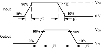
(1) The greater between
tr and tf is the same as tt.
Figure 6-3 Voltage Waveforms, Input
and Output Transition Times
(1) The
greater between tPLH and tPHL is the same as
tpd.
Figure 6-2 Voltage Waveforms
Propagation Delays