SLRS007C November 1986 – January 2015 SN754410
PRODUCTION DATA.
- 1 Features
- 2 Applications
- 3 Description
- 4 Simplified Schematic
- 5 Revision History
- 6 Pin Configuration and Functions
- 7 Specifications
- 8 Parameter Measurement Information
- 9 Detailed Description
- 10Application and Implementation
- 11Power Supply Recommendations
- 12Layout
- 13Device and Documentation Support
- 14Mechanical, Packaging, and Orderable Information
パッケージ・オプション
デバイスごとのパッケージ図は、PDF版データシートをご参照ください。
メカニカル・データ(パッケージ|ピン)
- NE|16
サーマルパッド・メカニカル・データ
発注情報
6 Pin Configuration and Functions
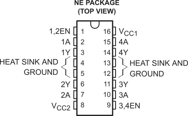
Pin Functions
| PIN | TYPE | DESCRIPTION | |
|---|---|---|---|
| NAME | NO. | ||
| 1,2EN | 1 | I | Enable driver channels 1 and 2 (active high input) |
| <1:4>A | 2, 7, 10, 15 | I | Driver inputs, non-inverting |
| <1:4>Y | 3, 6, 11, 14 | O | Driver outputs |
| GROUND | 4, 5, 12, 13 | — | Device ground and heat sink pin. Connect to circuit board ground plane with multiple solid vias |
| VCC2 | 8 | — | Power VCC for drivers 4.5V to 36V |
| 3,4EN | 9 | I | Enable driver channels 3 and 4 (active high input) |
| VCC1 | 16 | — | 5V supply for internal logic translation |