SLASE77A March 2016 – March 2016 TAS5733L
PRODUCTION DATA.
- 1 Features
- 2 Applications
- 3 Description
- 4 Revision History
- 5 Pin Configuration and Functions
-
6 Specifications
- 6.1 Absolute Maximum Ratings
- 6.2 ESD Ratings
- 6.3 Recommended Operating Conditions
- 6.4 Thermal Characteristics
- 6.5 Electrical Characteristics
- 6.6 Speaker Amplifier Characteristics
- 6.7 Protection Characteristics
- 6.8 Master Clock Characteristics
- 6.9 I²C Interface Timing Requirements
- 6.10 Serial Audio Port Timing Requirements
- 6.11 Typical Characteristics - Stereo BTL Mode
- 6.12 Typical Characteristics - Mono PBTL Mode
-
7 Detailed Description
- 7.1 Overview
- 7.2 Functional Block Diagram
- 7.3 Audio Signal Processing Overview
- 7.4 Feature Description
- 7.5 Device Functional Modes
- 7.6 Programming
- 7.7
Register Maps
- 7.7.1 Register Summary
- 7.7.2
Detailed Register Descriptions
- 7.7.2.1 Clock Control Register (0x00)
- 7.7.2.2 Device ID Register (0x01)
- 7.7.2.3 Error Status Register (0x02)
- 7.7.2.4 System Control Register 1 (0x03)
- 7.7.2.5 Serial Data Interface Register (0x04)
- 7.7.2.6 System Control Register 2 (0x05)
- 7.7.2.7 Soft Mute Register (0x06)
- 7.7.2.8 Volume Registers (0x07, 0x08, 0x09)
- 7.7.2.9 Volume Configuration Register (0x0E)
- 7.7.2.10 Modulation Limit Register (0x10)
- 7.7.2.11 Interchannel Delay Registers (0x11, 0x12, 0x13, and 0x14)
- 7.7.2.12 PWM Shutdown Group Register (0x19)
- 7.7.2.13 Start/Stop Period Register (0x1A)
- 7.7.2.14 Oscillator Trim Register (0x1B)
- 7.7.2.15 BKND_ERR Register (0x1C)
- 7.7.2.16 Input Multiplexer Register (0x20)
- 7.7.2.17 PWM Output MUX Register (0x25)
- 7.7.2.18 AGL Control Register (0x46)
- 7.7.2.19 PWM Switching Rate Control Register (0x4F)
- 7.7.2.20 Bank Switch and EQ Control (0x50)
-
8 Application and Implementation
- 8.1 Application Information
- 8.2
Typical Applications
- 8.2.1
Stereo Bridge Tied Load Application
- 8.2.1.1 Design Requirements
- 8.2.1.2 Detailed Design Procedure
- 8.2.1.3 Application Performance Plots
- 8.2.2 Mono Parallel Bridge Tied Load Application
- 8.2.1
Stereo Bridge Tied Load Application
- 9 Power Supply Recommendations
- 10Layout
- 11Device and Documentation Support
- 12Mechanical, Packaging, and Orderable Information
パッケージ・オプション
メカニカル・データ(パッケージ|ピン)
- DCA|48
サーマルパッド・メカニカル・データ
- DCA|48
発注情報
7 Detailed Description
7.1 Overview
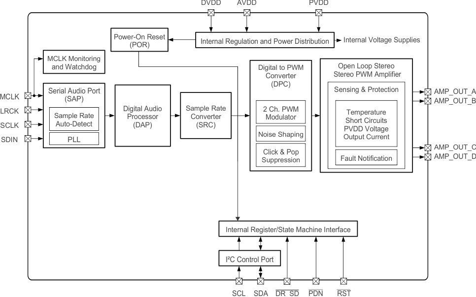
The TAS5733L device is an efficient, digital-input audio amplifier for driving stereo speakers configured as a bridge tied load (BTL). In parallel bridge tied load (PBTL) in can produce higher power by driving the parallel outputs into a single lower impedance load. One serial data input allows processing of up to two discrete audio channels and seamless integration to most digital audio processors and MPEG decoders. The device accepts a wide range of input data and data rates. A fully programmable data path routes these channels to the internal speaker drivers.
The TAS5733L device is a slave-only device receiving all clocks from external sources. The TAS5733L device operates with a PWM carrier between a 384-kHz switching rate and a 288-kHz switching rate, depending on the input sample rate. Oversampling combined with a fourth-order noise shaper provides a flat noise floor and excellent dynamic range from 20 Hz to 20 kHz.
7.2 Functional Block Diagram
7.3 Audio Signal Processing Overview
7.4 Feature Description
7.4.1 Clock, Autodetection, and PLL
The TAS5733L device is an I²S slave device. The TAS5733L device accepts MCLK, SCLK, and LRCK. The digital audio processor (DAP) supports all the sample rates and MCLK rates that are defined in the Clock Control Register.
The TAS5733L device checks to verify that SCLK is a specific value of 32 fS, 48 fS, or 64 fS. The DAP only supports a 1 × fS LRCK. The timing relationship of these clocks to SDIN is shown in subsequent sections. The clock section uses MCLK or the internal oscillator clock (when MCLK is unstable, out of range, or absent) to produce the internal clock (DCLK) running at 512 times the PWM switching frequency.
The DAP can autodetect and set the internal clock control logic to the appropriate settings for all supported clock rates as defined in the Clock Control Register.
The TAS5733L device has robust clock error handling that uses the built-in trimmed oscillator clock to quickly detect changes/errors. Once the system detects a clock change/error, the system mutes the audio (through a single-step mute) and then forces PLL to limp using the internal oscillator as a reference clock. Once the clocks are stable, the system autodetects the new rate and reverts to normal operation. During this process, the default volume is restored in a single step (also called hard unmute). The ramp process can be programmed to ramp back slowly (also called soft unmute) as defined in the Volume Configuration Register.
7.4.2 PWM Section
The TAS5733L DAP device uses noise-shaping and customized nonlinear correction algorithms to achieve high power efficiency and high-performance digital audio reproduction. The DAP uses a fourth-order noise shaper to increase dynamic range and SNR in the audio band. The PWM section accepts 24-bit PCM data from the DAP and outputs two BTL PWM audio output channels.
The PWM section has individual-channel dc-blocking filters that can be enabled and disabled. The filter cutoff frequency is less than 1 Hz.
The PWM section has an adjustable maximum modulation limit of 93.8% to 99.2%. For PVDD > 14.5 V the modulation index must be limited to 96.1% for safe and reliable operation.
7.4.3 PWM Level Meter
The structure in Figure 29 shows the PWM level meter that can be used to study the power profile.
 Figure 29. PWM Level Meter Structure
7.4.4 Automatic Gain Limiter (AGL)
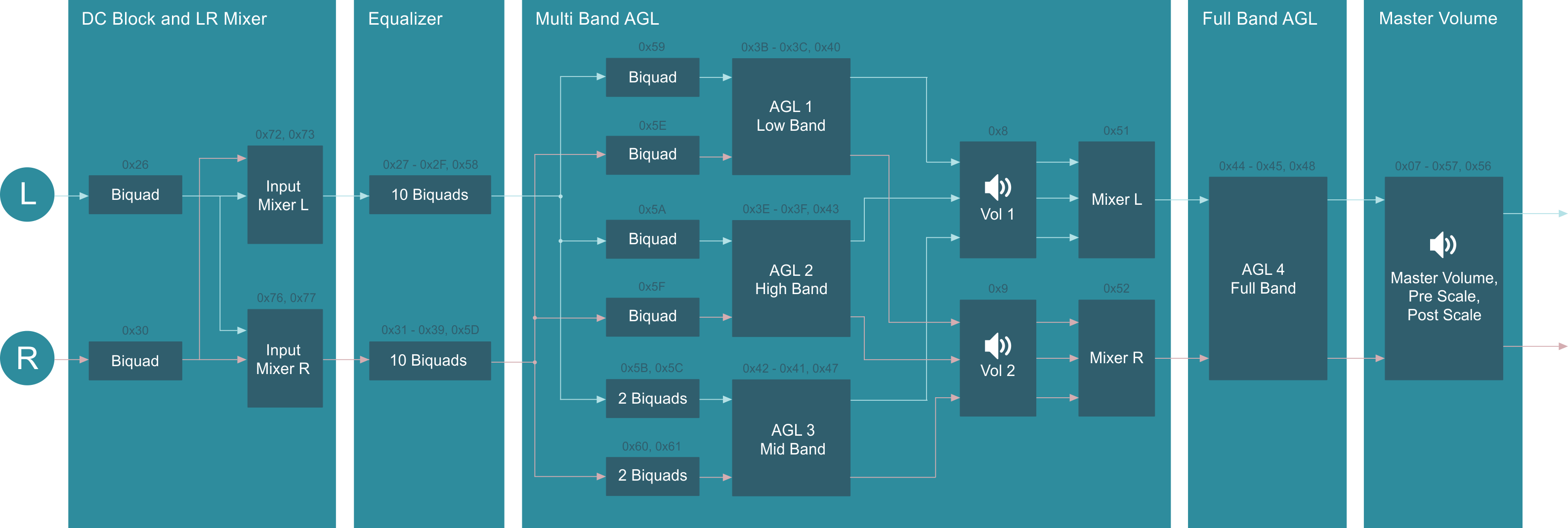
The AGL scheme has three AGL blocks. One ganged AGL exists for the high-band left/right channels, the mid-band left/right channels, and the low-band left/right channels.
The AGL input/output diagram is shown in Figure 30.
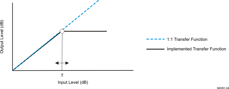
• Each AGL has adjustable threshold levels.
• Programmable attack and decay time constants
• Transparent compression: compressors can attack fast enough to avoid apparent clipping before engaging,
and decay times can be set slow enough to avoid pumping.
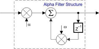
Table 1. AGL Structure
| α, ω | T | αa, ωa / αd, ωd | |
|---|---|---|---|
| AGL 1 | 0x3B | 0x40 | 0x3C |
| AGL 2 | 0x3E | 0x43 | 0x3F |
| AGL 3 | 0x47 | 0x41 | 0x42 |
| AGL 4 | 0x48 | 0x44 | 0x45 |
7.4.5 Fault Indication
ADR/FAULT is an input pin during power up. This pin can be programmed after RST to be an output by writing 1 to bit 0 of I²C register 0x05. In that mode, the ADR/FAULT pin has the definition shown in Table 2.
Any fault resulting in device shutdown is signaled by the ADR/FAULT pin going low (see Table 2). A latched version of this pin is available on D1 of register 0x02. This bit can be reset only by an I²C write.
Table 2. ADR/FAULT Output States
| ADR/FAULT | DESCRIPTION |
|---|---|
| 0 | Overcurrent (OC) or undervoltage (UVP) error or overtemperature error (OTE) or overvoltage error |
| 1 | No faults (normal operation) |
7.4.6 SSTIMER Pin Functionality
The SSTIMER pin uses a capacitor connected between this pin and ground to control the output duty cycle when exiting all-channel shutdown. The capacitor on the SSTIMER pin is slowly charged through an internal current source, and the charge time determines the rate at which the output transitions from a near-zero duty cycle to the desired duty cycle. This allows for a smooth transition that minimizes audible pops and clicks. When the part is shut down, the drivers are placed in the high-impedance state and transition slowly down through an internal 3-kΩ resistor, similarly minimizing pops and clicks. The shutdown transition time is independent of the SSTIMER pin capacitance. Larger capacitors increase the start-up time, while smaller capacitors decrease the start-up time. The SSTIMER pin can be left floating for BD modulation.
7.4.7 Device Protection System
7.4.7.1 Overcurrent (OC) Protection With Current Limiting
The TAS5733L device has independent, fast-reacting current detectors on all high-side and low-side power-stage FETs. The detector outputs are closely monitored to prevent the output current from increasing beyond the overcurrent threshold defined in the table.
If the output current increases beyond the overcurrent threshold, the device shuts down and the outputs transition to the off or high impedance (Hi-Z) state. The device returns to normal operation once the fault condition (i.e., a short circuit on the output) is removed. Current-limiting and overcurrent protection are not independent for half-bridges. That is, if the bridge-tied load between half-bridges A and B causes an overcurrent fault, half-bridges A, B, C, and D shut down.
7.4.7.2 Overtemperature Protection
The TAS5733L device has an overtemperature-protection system. If the device junction temperature exceeds 150°C (nominal), the device enters thermal shutdown, where all half-bridge outputs enter the high-impedance (Hi-Z) state, and ADR/FAULT asserts low if the device is configured to function as a fault output. The TAS5733L device recovers automatically once the junction temperature of the device drops approximately 30°C.
7.4.7.3 Undervoltage Protection (UVP) and Power-On Reset (POR)
The UVP and POR circuits of the TAS5733L device fully protect the device in any power-up/down and brownout situation. While powering up, the POR circuit resets the overload circuit (OLP) and ensures that all circuits are fully operational when the PVDD and AVDD supply voltages reach 7.6 V and 2.7 V, respectively. Although PVDD and AVDD are independently monitored. For PVDD, if the supply voltage drops below the UVP threshold, the protection feature immediately sets all half-bridge outputs to the high-impedance (Hi-Z) state and asserts ADR/FAULT low.
7.5 Device Functional Modes
The TAS5733L device is a digital input class-d amplifier with audio processing capabilities. The TAS5733L device has numerous modes to configure and control the device.
7.5.1 Serial Audio Port Operating Modes
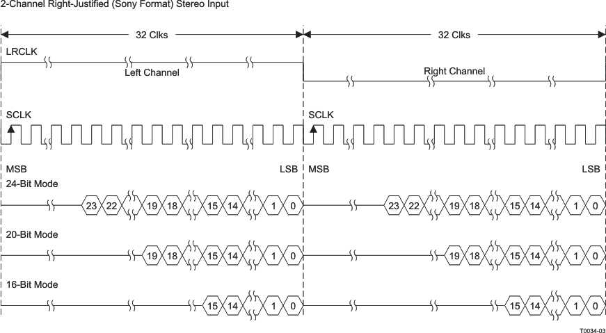
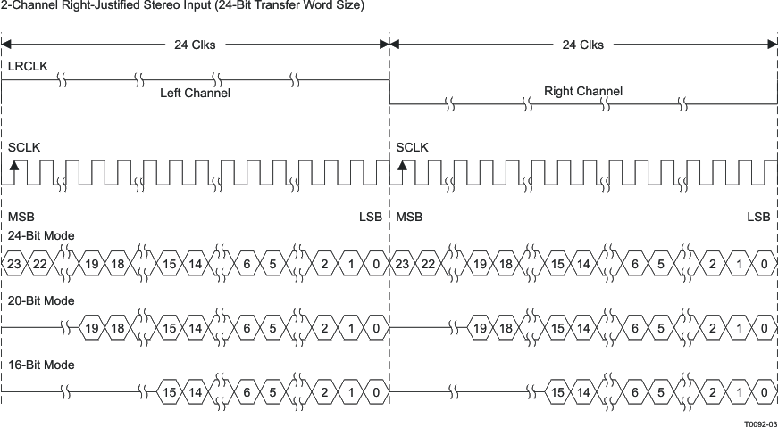
The serial audio port in the TAS5733L device supports industry-standard audio data formats, including I²S, Left-justified(LJ) and Right-justified(RJ) formats. To select the data format that will be used with the device can controlled by using the serial data interface registers 0x04. The default is 24bit, I²S mode. The timing diagrams for the various serial audio port are shown in the Serial Interface Control and Timing section
7.5.2 Communication Port Operating Modes
The TAS5733L device is configured via an I²C communication port. The I²C communication protocol is detailed in the 7.7 I²C Serial Control Port Requirements and Specifications section.
7.5.3 Speaker Amplifier Modes
The TAS5733L device can be configured as:
- Stereo Mode
- Mono Mode
7.5.3.1 Stereo Mode
Stereo mode is the most common option for the TAS5733L. TAS5733L can be connected in 2.0 mode to drive stereo channels. Detailed application section regarding the stereo mode is discussed in the Stereo Bridge Tied Load Application section.
7.5.3.2 Mono Mode
Mono mode is described as the operation where the two BTL outputs of amplifier are placed in parallel with one another to provide increase in the output power capability. This mode is typically used to drive subwoofers, which require more power to drive larger loudspeakers with high-amplitude, low-frequency energy. Detailed application section regarding the mono mode is discussed in the Mono Parallel Bridge Tied Load Application section.
7.6 Programming
7.6.1 I²C Serial Control Interface
The TAS5733L device has a bidirectional I²C interface that is compatible with the Inter IC (I²C) bus protocol and supports both 100-kHz and 400-kHz data transfer rates for single- and multiple-byte write and read operations. This is a slave-only device that does not support a multimaster bus environment or wait-state insertion. The control interface is used to program the registers of the device and to read device status.
The DAP supports the standard-mode I²C bus operation (100 kHz maximum) and the fast I²C bus operation (400 kHz maximum). The DAP performs all I²C operations without I²C wait cycles.
7.6.1.1 General I²C Operation
The I²C bus employs two signals, SDA (data) and SCL (clock), to communicate between integrated circuits in a system. Data is transferred on the bus serially, one bit at a time. The address and data can be transferred in byte (8-bit) format, with the most-significant bit (MSB) transferred first. In addition, each byte transferred on the bus is acknowledged by the receiving device with an acknowledge bit. Each transfer operation begins with the master device driving a start condition on the bus and ends with the master device driving a stop condition on the bus. The bus uses transitions on the data pin (SDA) while the clock is high to indicate start and stop conditions. A high-to-low transition on SDA indicates a start and a low-to-high transition indicates a stop. Normal data-bit transitions must occur within the low time of the clock period. These conditions are shown in Figure 32. The master generates the 7-bit slave address and the read/write (R/W) bit to open communication with another device and then waits for an acknowledge condition. The TAS5733L device holds SDA low during the acknowledge clock period to indicate an acknowledgment. When this occurs, the master transmits the next byte of the sequence. Each device is addressed by a unique 7-bit slave address plus R/W bit (1 byte). All compatible devices share the same signals via a bidirectional bus using a wired-AND connection. An external pullup resistor must be used for the SDA and SCL signals to set the high level for the bus.
 Figure 32. Typical I²C Sequence
No limit exists for the number of bytes that can be transmitted between start and stop conditions. When the last word transfers, the master generates a stop condition to release the bus. A generic data transfer sequence is shown in Figure 32.
The 7-bit address for the TAS5733L device is 0101 010 (0x54) or 0101 011 (0x56) as defined by ADR/FAULT (external pulldown for 0x54 and pullup for 0x56).
7.6.1.2 I²C Slave Address
The ADR/FAULT is an input pin during power-up and after each toggle of RST, which is used to set the I²C sub-address of the device. The ADR/FAULT can also operate as a fault output after power-up is complete and the address has been latched in.
At power-up, and after each toggle of RST, the pin is read to determine its voltage level. If the pin is left floating, an internal pull-up will set the I²C sub-address to 0x56. This will also be the case if an external resistor is used to pull the pin up to AVDD. To set the sub-address to 0x54, an external resistor (specified in Typical Applications) must be connected to the system ground.
As mentioned, the pin can also be reconfigured as an output driver via I²C for fault monitoring. Use System Control Register 2 (0x05) to set ADR/FAULT pin to be used as a fault output during fault conditions.
I²C Device Address Change Procedure
- Write to device address change enable register, 0xF8 with a value of 0xF9A5 A5A5.
- Write to device register 0xF9 with a value of 0x0000 00XX, where XX is the new address.
- Any writes after that should use the new device address XX.
7.6.1.3 Single- and Multiple-Byte Transfers
The serial control interface supports both single-byte and multiple-byte read/write operations for subaddresses 0x00 to 0x1F. However, for the subaddresses 0x20 to 0xFF, the serial control interface supports only multiple-byte read/write operations (in multiples of 4 bytes).
During multiple-byte read operations, the DAP responds with data, a byte at a time, starting at the subaddress assigned, as long as the master device continues to respond with acknowledges. If a particular subaddress does not contain 32 bits, the unused bits are read as logic 0.
During multiple-byte write operations, the DAP compares the number of bytes transmitted to the number of bytes that are required for each specific subaddress. For example, if a write command is received for a biquad subaddress, the DAP must receive five 32-bit words. If fewer than five 32-bit data words have been received when a stop command (or another start command) is received, the received data is discarded.
Supplying a subaddress for each subaddress transaction is referred to as random I²C addressing. The TAS5733L device also supports sequential I²C addressing. For write transactions, if a subaddress is issued followed by data for that subaddress and the 15 subaddresses that follow, a sequential I²C write transaction has taken place, and the data for all 16 subaddresses is successfully received by the TAS5733L device. For I²C sequential-write transactions, the subaddress then serves as the start address, and the amount of data subsequently transmitted before a stop or start is transmitted determines how many subaddresses are written. As was true for random addressing, sequential addressing requires that a complete set of data be transmitted. If only a partial set of data is written to the last subaddress, the data for the last subaddress is discarded. However, all other data written is accepted; only the incomplete data is discarded.
7.6.1.4 Single-Byte Write
As shown in Figure 33, a single-byte data-write transfer begins with the master device transmitting a start condition followed by the I²C device address and the read/write bit. The read/write bit determines the direction of the data transfer. For a data-write transfer, the read/write bit is a 0. After receiving the correct I²C device address and the read/write bit, the DAP responds with an acknowledge bit. Next, the master transmits the address byte or bytes corresponding to the internal memory address being accessed. After receiving the address byte, the TAS5733L device again responds with an acknowledge bit. Next, the master device transmits the data byte to be written to the memory address being accessed. After receiving the data byte, the TAS5733L device again responds with an acknowledge bit. Finally, the master device transmits a stop condition to complete the single-byte data-write transfer.
 Figure 33. Single-Byte Write Transfer
7.6.1.5 Multiple-Byte Write
A multiple-byte data-write transfer is identical to a single-byte data-write transfer except that multiple data bytes are transmitted by the master device to the DAP as shown in Figure 34. After receiving each data byte, the TAS5733L device responds with an acknowledge bit.
 Figure 34. Multiple-Byte Write Transfer
7.6.1.6 Single-Byte Read
As shown in Figure 35, a single-byte data-read transfer begins with the master device transmitting a start condition, followed by the I²C device address and the read/write bit. For the data read transfer, both a write followed by a read are actually done. Initially, a write is done to transfer the address byte or bytes of the internal memory address to be read. As a result, the read/write bit becomes a 0. After receiving the TAS5733L address and the read/write bit, TAS5733L device responds with an acknowledge bit. In addition, after sending the internal memory address byte or bytes, the master device transmits another start condition followed by the TAS5733L address and the read/write bit again. This time, the read/write bit becomes a 1, indicating a read transfer. After receiving the address and the read/write bit, the TAS5733L device again responds with an acknowledge bit. Next, the TAS5733L device transmits the data byte from the memory address being read. After receiving the data byte, the master device transmits a not-acknowledge followed by a stop condition to complete the single-byte data-read transfer.
 Figure 35. Single-Byte Read Transfer
7.6.1.7 Multiple-Byte Read
A multiple-byte data-read transfer is identical to a single-byte data-read transfer except that multiple data bytes are transmitted by the TAS5733L device to the master device as shown in Figure 36. Except for the last data byte, the master device responds with an acknowledge bit after receiving each data byte.
 Figure 36. Multiple-Byte Read Transfer
7.6.2 Serial Interface Control and Timing
7.6.2.1 Serial Data Interface
Serial data is input on SDIN. The PWM outputs are derived from SDIN. The TAS5733L DAP accepts serial data in 16-bit, 20-bit, or 24-bit left-justified, right-justified, and I²S serial data formats.
7.6.2.2 I²S Timing
I²S timing uses LRCK to define when the data being transmitted is for the left channel and when the data is for the right channel. LRCK is low for the left channel and high for the right channel. A bit clock running at 32 × fS, 48 × fS, or 64 × fS is used to clock in the data. A delay of one bit clock exists from the time the LRCK signal changes state to the first bit of data on the data lines. The data is written MSB-first and is valid on the rising edge of bit clock. The DAP masks unused trailing data bit positions.
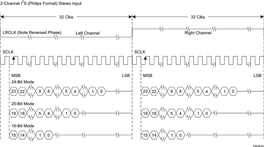
NOTE:
All data presented in two's-complement form with MSB first.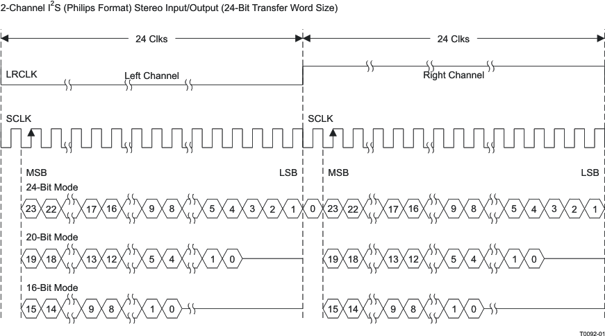
NOTE:
All data presented in two's-complement form with MSB first.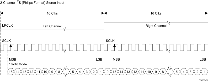
NOTE:
All data presented in two's-complement form with MSB first.7.6.2.3 Left-Justified
Left-justified (LJ) timing uses LRCK to define when the data being transmitted is for the left channel and when the data is for the right channel. LRCK is high for the left channel and low for the right channel. A bit clock running at 32 × fS, 48 × fS, or 64 × fS is used to clock in the data. The first bit of data appears on the data lines at the same time LRCK toggles. The data is written MSB-first and is valid on the rising edge of the bit clock. The DAP masks unused trailing data bit positions.
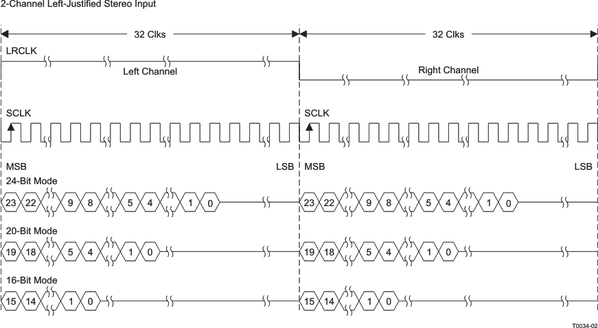
NOTE:
All data presented in two's-complement form with MSB first.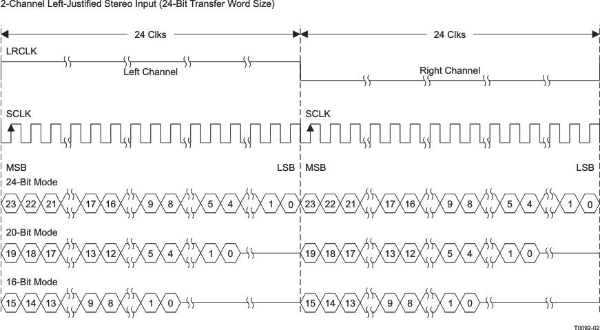
NOTE:
All data presented in two's-complement form with MSB first.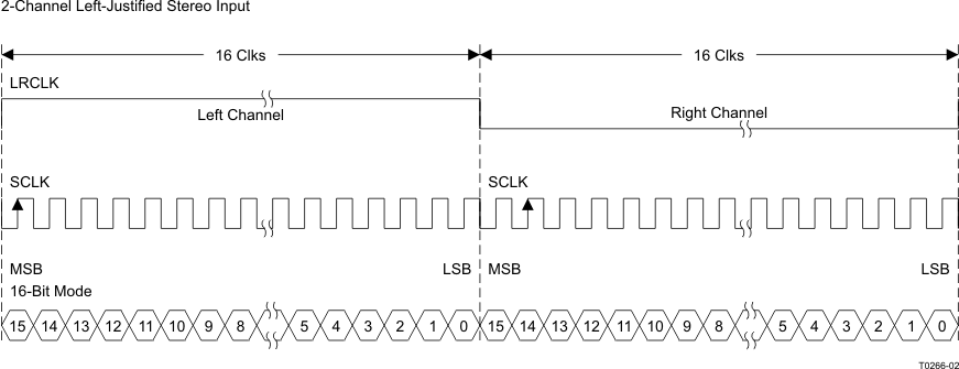
NOTE:
All data presented in two's-complement form with MSB first.7.6.2.4 Right-Justified
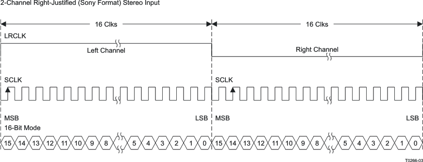
Right-justified (RJ) timing uses LRCK to define when the data being transmitted is for the left channel and when the data is for the right channel. LRCK is high for the left channel and low for the right channel. A bit clock running at 32 × fS, 48 × fS, or 64 × fS is used to clock in the data. The first bit of data appears on the data 8 bit-clock periods (for 24-bit data) after LRCK toggles. In RJ mode, the LSB of data is always clocked by the last bit clock before LRCK transitions. The data is written MSB-first and is valid on the rising edge of bit clock. The DAP masks unused leading data bit positions.
7.6.3 26-Bit 3.23 Number Format
All mixer gain coefficients are 26-bit coefficients using a 3.23 number format. Numbers formatted as 3.23 numbers mean that the binary point has 3 bits to the left and 23 bits to the right. This is shown in Figure 46.
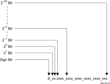 Figure 46. 3.23 Format
The decimal value of a 3.23 format number can be found by following the weighting shown in Figure 46. If the most significant bit is logic 0, the number is a positive number, and the weighting shown yields the correct number. If the most significant bit is a logic 1, then the number is a negative number. In the case every bit must be inverted, a 1 added to the result, and then the weighting shown in Figure 47 applies to obtain the magnitude of the negative number.
 Figure 47. Conversion Weighting Factors—3.23 Format to Floating Point
Gain coefficients, entered via the I²C bus, must be entered as 32-bit binary numbers. The format of the 32-bit number (4-byte or 8-digit hexadecimal number) is shown in Figure 48.
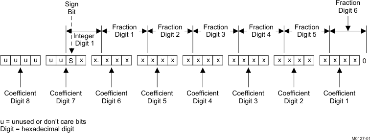 Figure 48. Alignment of 3.23 Coefficient in 32-Bit I²C Word
Table 3. Sample Calculation for 3.23 Format
| db | Linear | Decimal | Hex (3.23 Format) |
|---|---|---|---|
| 0 | 1 | 8,388,608 | 80 0000 |
| 5 | 1.77 | 14,917,288 | 00E3 9EA8 |
| –5 | 0.56 | 4,717,260 | 0047 FACC |
| X | L = 10(X / 20) | D = 8,388,608 × L | H = dec2hex (D, 8) |
Table 4. Sample Calculation for 9.17 Format
| db | Linear | Decimal | Hex (9.17 Format) |
|---|---|---|---|
| 0 | 1 | 131,072 | 2 0000 |
| 5 | 1.77 | 231,997 | 3 8A3D |
| –5 | 0.56 | 73,400 | 1 1EB8 |
| X | L = 10(X / 20) | D = 131,072 × L | H = dec2hex (D, 8) |
7.7 Register Maps
7.7.1 Register Summary
| SUBADDRESS | REGISTER NAME | NO. OF BYTES | CONTENTS | DEFAULT VALUE |
|---|---|---|---|---|
| A u indicates unused bits. | ||||
| 0x00 | Clock control register | 1 | Description shown in subsequent section | 0x6C |
| 0x01 | Device ID register | 1 | Description shown in subsequent section | 0x40 |
| 0x02 | Error status register | 1 | Description shown in subsequent section | 0x00 |
| 0x03 | System control register 1 | 1 | Description shown in subsequent section | 0xA0 |
| 0x04 | Serial data interface register | 1 | Description shown in subsequent section | 0x05 |
| 0x05 | System control register 2 | 1 | Description shown in subsequent section | 0x40 |
| 0x06 | Soft mute register | 1 | Description shown in subsequent section | 0x00 |
| 0x07 | Master volume | 2 | Description shown in subsequent section | 0x03FF (mute) |
| 0x08 | Channel 1 vol | 2 | Description shown in subsequent section | 0x00C0 (0 dB) |
| 0x09 | Channel 2 vol | 2 | Description shown in subsequent section | 0x00C0 (0 dB) |
| 0x0A | Channel 3 vol | 2 | Description shown in subsequent section | 0x00C0 (0 dB) |
| 0x0B | Reserved | 2 | Reserved(1) | 0x03FF |
| 0x0C | 2 | Reserved(1) | 0x00C0 | |
| 0x0D | 1 | Reserved(1) | 0xC0 | |
| 0x0E | Volume configuration register | 1 | Description shown in subsequent section | 0xF0 |
| 0x0F | Reserved | 1 | Reserved(1) | 0x97 |
| 0x10 | Modulation limit register | 1 | Description shown in subsequent section | 0x01 |
| 0x11 | IC delay channel 1 | 1 | Description shown in subsequent section | 0xAC |
| 0x12 | IC delay channel 2 | 1 | Description shown in subsequent section | 0x54 |
| 0x13 | IC delay channel 3 | 1 | Description shown in subsequent section | 0xAC |
| 0x14 | IC delay channel 4 | 1 | Description shown in subsequent section | 0x54 |
| 0x15 | Reserved | 1 | Reserved(1) | 0xAC |
| 0x16 | 0x54 | |||
| 0x17 | 0x00 | |||
| 0x18 | PWM Start | 0x0F | ||
| 0x19 | PWM Shutdown Group Register | 1 | Description shown in subsequent section | 0x30 |
| 0x1A | Start/stop period register | 1 | Description shown in subsequent section | 0x68 |
| 0x1B | Oscillator trim register | 1 | Description shown in subsequent section | 0x82 |
| 0x1C | BKND_ERR register | 1 | Description shown in subsequent section | 0x57 |
| 0x1D–0x1F | 1 | Reserved(1) | 0x00 | |
| 0x20 | Input MUX register | 4 | Description shown in subsequent section | 0x0001 7772 |
| 0x21 | Reserved | 4 | Reserved(1) | 0x0000 4303 |
| 0x22 | 4 | 0x0000 0000 | ||
| 0x23 | 4 | 0x0000 0000 | ||
| 0x24 | 4 | 0x0000 0000 | ||
| 0x25 | PWM MUX register | 4 | Description shown in subsequent section | 0x0102 1345 |
| 0x26 | ch1_bq[0] | 20 | u[31:26], b0[25:0] | 0x0080 0000 |
| u[31:26], b1[25:0] | 0x0000 0000 | |||
| u[31:26], b2[25:0] | 0x0000 0000 | |||
| u[31:26], a1[25:0] | 0x0000 0000 | |||
| u[31:26], a2[25:0] | 0x0000 0000 | |||
| 0x27 | ch1_bq[1] | 20 | u[31:26], b0[25:0] | 0x0080 0000 |
| u[31:26], b1[25:0] | 0x0000 0000 | |||
| u[31:26], b2[25:0] | 0x0000 0000 | |||
| u[31:26], a1[25:0] | 0x0000 0000 | |||
| u[31:26], a2[25:0] | 0x0000 0000 | |||
| 0x28 | ch1_bq[2] | 20 | u[31:26], b0[25:0] | 0x0080 0000 |
| u[31:26], b1[25:0] | 0x0000 0000 | |||
| u[31:26], b2[25:0] | 0x0000 0000 | |||
| u[31:26], a1[25:0] | 0x0000 0000 | |||
| u[31:26], a2[25:0] | 0x0000 0000 | |||
| 0x29 | ch1_bq[3] | 20 | u[31:26], b0[25:0] | 0x0080 0000 |
| u[31:26], b1[25:0] | 0x0000 0000 | |||
| u[31:26], b2[25:0] | 0x0000 0000 | |||
| u[31:26], a1[25:0] | 0x0000 0000 | |||
| u[31:26], a2[25:0] | 0x0000 0000 | |||
| 0x2A | ch1_bq[4] | 20 | u[31:26], b0[25:0] | 0x0080 0000 |
| u[31:26], b1[25:0] | 0x0000 0000 | |||
| u[31:26], b2[25:0] | 0x0000 0000 | |||
| u[31:26], a1[25:0] | 0x0000 0000 | |||
| u[31:26], a2[25:0] | 0x0000 0000 | |||
| 0x2B | ch1_bq[5] | 20 | u[31:26], b0[25:0] | 0x0080 0000 |
| u[31:26], b1[25:0] | 0x0000 0000 | |||
| u[31:26], b2[25:0] | 0x0000 0000 | |||
| u[31:26], a1[25:0] | 0x0000 0000 | |||
| u[31:26], a2[25:0] | 0x0000 0000 | |||
| 0x2C | ch1_bq[6] | 20 | u[31:26], b0[25:0] | 0x0080 0000 |
| u[31:26], b1[25:0] | 0x0000 0000 | |||
| u[31:26], b2[25:0] | 0x0000 0000 | |||
| u[31:26], a1[25:0] | 0x0000 0000 | |||
| u[31:26], a2[25:0] | 0x0000 0000 | |||
| 0x2D | ch1_bq[7] | 20 | u[31:26], b0[25:0] | 0x0080 0000 |
| u[31:26], b1[25:0] | 0x0000 0000 | |||
| u[31:26], b2[25:0] | 0x0000 0000 | |||
| u[31:26], a1[25:0] | 0x0000 0000 | |||
| u[31:26], a2[25:0] | 0x0000 0000 | |||
| 0x2E | ch1_bq[8] | 20 | u[31:26], b0[25:0] | 0x0080 0000 |
| u[31:26], b1[25:0] | 0x0000 0000 | |||
| u[31:26], b2[25:0] | 0x0000 0000 | |||
| u[31:26], a1[25:0] | 0x0000 0000 | |||
| u[31:26], a2[25:0] | 0x0000 0000 | |||
| 0x2F | ch1_bq[9] | 20 | u[31:26], b0[25:0] | 0x0080 0000 |
| u[31:26], b1[25:0] | 0x0000 0000 | |||
| u[31:26], b2[25:0] | 0x0000 0000 | |||
| u[31:26], a1[25:0] | 0x0000 0000 | |||
| u[31:26], a2[25:0] | 0x0000 0000 | |||
| 0x30 | ch2_bq[0] | 20 | u[31:26], b0[25:0] | 0x0080 0000 |
| u[31:26], b1[25:0] | 0x0000 0000 | |||
| u[31:26], b2[25:0] | 0x0000 0000 | |||
| u[31:26], a1[25:0] | 0x0000 0000 | |||
| u[31:26], a2[25:0] | 0x0000 0000 | |||
| 0x31 | ch2_bq[1] | 20 | u[31:26], b0[25:0] | 0x0080 0000 |
| u[31:26], b1[25:0] | 0x0000 0000 | |||
| u[31:26], b2[25:0] | 0x0000 0000 | |||
| u[31:26], a1[25:0] | 0x0000 0000 | |||
| u[31:26], a2[25:0] | 0x0000 0000 | |||
| 0x32 | ch2_bq[2] | 20 | u[31:26], b0[25:0] | 0x0080 0000 |
| u[31:26], b1[25:0] | 0x0000 0000 | |||
| u[31:26], b2[25:0] | 0x0000 0000 | |||
| u[31:26], a1[25:0] | 0x0000 0000 | |||
| u[31:26], a2[25:0] | 0x0000 0000 | |||
| 0x33 | ch2_bq[3] | 20 | u[31:26], b0[25:0] | 0x0080 0000 |
| u[31:26], b1[25:0] | 0x0000 0000 | |||
| u[31:26], b2[25:0] | 0x0000 0000 | |||
| u[31:26], a1[25:0] | 0x0000 0000 | |||
| u[31:26], a2[25:0] | 0x0000 0000 | |||
| 0x34 | ch2_bq[4] | 20 | u[31:26], b0[25:0] | 0x0080 0000 |
| u[31:26], b1[25:0] | 0x0000 0000 | |||
| u[31:26], b2[25:0] | 0x0000 0000 | |||
| u[31:26], a1[25:0] | 0x0000 0000 | |||
| u[31:26], a2[25:0] | 0x0000 0000 | |||
| 0x35 | ch2_bq[5] | 20 | u[31:26], b0[25:0] | 0x0080 0000 |
| u[31:26], b1[25:0] | 0x0000 0000 | |||
| u[31:26], b2[25:0] | 0x0000 0000 | |||
| u[31:26], a1[25:0] | 0x0000 0000 | |||
| u[31:26], a2[25:0] | 0x0000 0000 | |||
| 0x36 | ch2_bq[6] | 20 | u[31:26], b0[25:0] | 0x0080 0000 |
| u[31:26], b1[25:0] | 0x0000 0000 | |||
| u[31:26], b2[25:0] | 0x0000 0000 | |||
| u[31:26], a1[25:0] | 0x0000 0000 | |||
| u[31:26], a2[25:0] | 0x0000 0000 | |||
| 0x37 | ch2_bq[7] | 20 | u[31:26], b0[25:0] | 0x0080 0000 |
| u[31:26], b1[25:0] | 0x0000 0000 | |||
| u[31:26], b2[25:0] | 0x0000 0000 | |||
| u[31:26], a1[25:0] | 0x0000 0000 | |||
| u[31:26], a2[25:0] | 0x0000 0000 | |||
| 0x38 | ch2_bq[8] | 20 | u[31:26], b0[25:0] | 0x0080 0000 |
| u[31:26], b1[25:0] | 0x0000 0000 | |||
| u[31:26], b2[25:0] | 0x0000 0000 | |||
| u[31:26], a1[25:0] | 0x0000 0000 | |||
| u[31:26], a2[25:0] | 0x0000 0000 | |||
| 0x39 | ch2_bq[9] | 20 | u[31:26], b0[25:0] | 0x0080 0000 |
| u[31:26], b1[25:0] | 0x0000 0000 | |||
| u[31:26], b2[25:0] | 0x0000 0000 | |||
| u[31:26], a1[25:0] | 0x0000 0000 | |||
| u[31:26], a2[25:0] | 0x0000 0000 | |||
| 0x3A | Reserved | 4 | Reserved(1) | 0x0080 0000 0000 0000 |
| 0x3B | AGL1 softening filter alpha | 8 | u[31:26], ae[25:0] | 0x0008 0000 |
| AGL1 softening filter omega | u[31:26], oe[25:0] | 0x0078 0000 | ||
| 0x3C | AGL1 attack rate | 8 | Description shown in subsequent section | 0x0000 0100 |
| AGL1 release rate | Description shown in subsequent section | 0xFFFF FF00 | ||
| 0x3D | 8 | Reserved(1) | ||
| 0x3E | AGL2 softening filter alpha | 8 | u[31:26], ae[25:0] | 0x0008 0000 |
| AGL2 softening filter omega | u[31:26], oe[25:0] | 0x0078 0000 | ||
| 0x3F | AGL2 attack rate | 8 | u[31:26], at[25:0] | 0x0008 0000 |
| AGL2 release rate | u[31:26], rt[25:0] | 0xFFF8 0000 | ||
| 0x40 | AGL1 attack threshold | 4 | T1[31:0] (9.23 format) | 0x0800 0000 |
| 0x41 | AGL3 attack threshold | 4 | T1[31:0] (9.23 format) | 0x0074 0000 |
| 0x42 | AGL3 attack rate | 8 | Description shown in subsequent section | 0x0008 0000 |
| AGL3 release rate | Description shown in subsequent section | 0xFFF8 0000 | ||
| 0x43 | AGL2 attack threshold | 4 | T2[31:0] (9.23 format) | 0x0074 0000 |
| 0x44 | AGL4 attack threshold | 4 | T1[31:0] (9.23 format) | 0x0074 0000 |
| 0x45 | AGL4 attack rate | 8 | 0x0008 0000 | |
| AGL4 release rate | 0xFFF8 0000 | |||
| 0x46 | AGL control | 4 | Description shown in subsequent section | 0x0002 0000 |
| 0x47 | AGL3 softening filter alpha | 8 | u[31:26], ae[25:0] | 0x0008 0000 |
| AGL3 softening filter omega | u[31:26], oe[25:0] | 0x0078 0000 | ||
| 0x48 | AGL4 softening filter alpha | 8 | u[31:26], ae[25:0] | 0x0008 0000 |
| AGL4 softening filter omega | u[31:26], oe[25:0] | 0x0078 0000 | ||
| 0x49 | Reserved | 4 | Reserved(1) | |
| 0x4A | 4 | 0x1212 1010 E1FF FFFF F95E 1212 | ||
| 0x4B | 4 | 0x0000 296E | ||
| 0x4C | 4 | 0x0000 5395 | ||
| 0x4D | 4 | 0x0000 0000 | ||
| 0x4E | 4 | 0x0000 0000 | ||
| 0x4F | PWM switching rate control | 4 | u[31:4], src[3:0] | 0x0000 0008 |
| 0x50 | Bank switch control | 4 | Description shown in subsequent section | 0x0F70 8000 |
| 0x51 | Ch 1 output mixer | 12 | Ch 1 output mix1[2] | 0x0080 0000 |
| Ch 1 output mix1[1] | 0x0000 0000 | |||
| Ch 1 output mix1[0] | 0x0000 0000 | |||
| 0x52 | Ch 2 output mixer | 12 | Ch 2 output mix2[2] | 0x0080 0000 |
| Ch 2 output mix2[1] | 0x0000 0000 | |||
| Ch 2 output mix2[0] | 0x0000 0000 | |||
| 0x53 | 16 | Reserved(1) | 0x0080 0000 0000 0000 0000 0000 | |
| 0x54 | 16 | Reserved(1) | 0x0080 0000 0000 0000 0000 0000 | |
| 0x56 | Output post-scale | 4 | u[31:26], post[25:0] | 0x0080 0000 |
| 0x57 | Output pre-scale | 4 | u[31:26], pre[25:0] (9.17 format) | 0x0002 0000 |
| 0x58 | ch1_bq[10] | 20 | u[31:26], b0[25:0] | 0x0080 0000 |
| u[31:26], b1[25:0] | 0x0000 0000 | |||
| u[31:26], b2[25:0] | 0x0000 0000 | |||
| u[31:26], a1[25:0] | 0x0000 0000 | |||
| u[31:26], a2[25:0] | 0x0000 0000 | |||
| 0x59 | ch1_cross_bq[0] | 20 | u[31:26], b0[25:0] | 0x0080 0000 |
| ch1_cross_bq[1] | 0x0000 0000 | |||
| ch1_cross_bq[2] | 0x0000 0000 | |||
| u[31:26], a1[25:0] | 0x0000 0000 | |||
| u[31:26], a2[25:0] | 0x0000 0000 | |||
| 0x5A | ch1_cross_bq[1] | 20 | u[31:26], b0[25:0] | 0x0080 0000 |
| u[31:26], b1[25:0] | 0x0000 0000 | |||
| u[31:26], b2[25:0] | 0x0000 0000 | |||
| u[31:26], a1[25:0] | 0x0000 0000 | |||
| u[31:26], a2[25:0] | 0x0000 0000 | |||
| 0x5B | ch1_cross_bq[2] | 20 | u[31:26], b0[25:0] | 0x0080 0000 |
| u[31:26], b1[25:0] | 0x0000 0000 | |||
| u[31:26], b2[25:0] | 0x0000 0000 | |||
| u[31:26], a1[25:0] | 0x0000 0000 | |||
| u[31:26], a2[25:0] | 0x0000 0000 | |||
| 0x5C | ch1_cross_bq[3] | 20 | u[31:26], b0[25:0] | 0x0080 0000 |
| u[31:26], b1[25:0] | 0x0000 0000 | |||
| u[31:26], b2[25:0] | 0x0000 0000 | |||
| u[31:26], a1[25:0] | 0x0000 0000 | |||
| u[31:26], a2[25:0] | 0x0000 0000 | |||
| 0x5D | ch2_bq[10] | 20 | u[31:26], b0[25:0] | 0x0080 0000 |
| u[31:26], b1[25:0] | 0x0000 0000 | |||
| u[31:26], b2[25:0] | 0x0000 0000 | |||
| u[31:26], a1[25:0] | 0x0000 0000 | |||
| u[31:26], a2[25:0] | 0x0000 0000 | |||
| 0x5E | ch2_cross_bq[0] | 20 | u[31:26], b0[25:0] | 0x0080 0000 |
| u[31:26], b1[25:0] | 0x0000 0000 | |||
| u[31:26], b2[25:0] | 0x0000 0000 | |||
| u[31:26], a1[25:0] | 0x0000 0000 | |||
| u[31:26], a2[25:0] | 0x0000 0000 | |||
| 0x5F | ch2_cross_bq[1] | 20 | u[31:26], b0[25:0] | 0x0080 0000 |
| u[31:26], b1[25:0] | 0x0000 0000 | |||
| u[31:26], b2[25:0] | 0x0000 0000 | |||
| u[31:26], a1[25:0] | 0x0000 0000 | |||
| u[31:26], a2[25:0] | 0x0000 0000 | |||
| 0x60 | ch2_cross_bq[2] | 20 | u[31:26], b0[25:0] | 0x0080 0000 |
| u[31:26], b1[25:0] | 0x0000 0000 | |||
| u[31:26], b2[25:0] | 0x0000 0000 | |||
| u[31:26], a1[25:0] | 0x0000 0000 | |||
| u[31:26], a2[25:0] | 0x0000 0000 | |||
| 0x61 | ch2_cross_bq[3] | 20 | u[31:26], b0[25:0] | 0x0080 0000 |
| u[31:26], b1[25:0] | 0x0000 0000 | |||
| u[31:26], b2[25:0] | 0x0000 0000 | |||
| u[31:26], a1[25:0] | 0x0000 0000 | |||
| u[31:26], a2[25:0] | 0x0000 0000 | |||
| 0x62 | IDF post scale | 4 | Description shown in subsequent section | 0x0000 0080 |
| 0x63–0x69 | Reserved | 4 | Reserved(1) | 0x0000 0000 |
| 0x6A | 4 | 0x0000 8312 | ||
| 0x6B | Left channel PWM level meter | 4 | Data[31:0] | 0x007F 7CED |
| 0x6C | Right channel PWM level meter | 4 | Data[31:0] | 0x0000 0000 |
| 0x6D | Reserved | 8 | Reserved(1) | 0x0000 0000 0000 0000 |
| 0x6E–0x6F | 4 | 0x0000 0000 | ||
| 0x70 | ch1 inline mixer | 4 | u[31:26], in_mix1[25:0] | 0x0080 0000 |
| 0x71 | inline_AGL_en_mixer_ch1 | 4 | u[31:26], in_mixagl_1[25:0] | 0x0000 0000 |
| 0x72 | ch1 right_channel mixer | 4 | u[31:26], right_mix1[25:0] | 0x0000 0000 |
| 0x73 | ch1 left_channel_mixer | 4 | u[31:26], left_mix_1[25:0] | 0x0080 0000 |
| 0x74 | ch2 inline mixer | 4 | u[31:26], in_mix2[25:0] | 0x0080 0000 |
| 0x75 | inline_AGL_en_mixer_ch2 | 4 | u[31:26], in_mixagl_2[25:0] | 0x0000 0000 |
| 0x76 | ch2 left_chanel mixer | 4 | u[31:26], left_mix1[25:0] | 0x0000 0000 |
| 0x77 | ch2 right_channel_mixer | 4 | u[31:26], right_mix_1[25:0] | 0x0080 0000 |
| 0x78–0xF7 | Reserved(1) | 0x0000 0000 | ||
| 0xF8 | Update device address key | 4 | Dev Id Update Key[31:0] (Key = 0xF9A5A5A5) | 0x0000 0054 |
| 0xF9 | Update device address | 4 | u[31:8],New Dev Id[7:0] (New Dev Id = 0x54 for TAS5733L) | 0x0000 0054 |
| 0xFA–0xFF | 4 | Reserved(1) | 0x0000 0000 |
All DAP coefficients are 3.23 format unless specified otherwise.
Registers 0x3B through 0x46 should be altered only during the initialization phase.
7.7.2 Detailed Register Descriptions
7.7.2.1 Clock Control Register (0x00)
The clocks and data rates are automatically determined by the TAS5733L. The clock control register contains the autodetected clock status. Bits D7–D5 reflect the sample rate. Bits D4–D2 reflect the MCLK frequency.
Table 5. Clock Control Register (0x00)
| D7 | D6 | D5 | D4 | D3 | D2 | D1 | D0 | FUNCTION |
|---|---|---|---|---|---|---|---|---|
| 0 | 0 | 0 | – | – | – | – | – | fS = 32-kHz sample rate |
| 0 | 0 | 1 | – | – | – | – | – | Reserved |
| 0 | 1 | 0 | – | – | – | – | – | Reserved |
| 0 | 1 | 1 | – | – | – | – | – | fS = 44.1/48-kHz sample rate(1) |
| 1 | 0 | 0 | – | – | – | – | – | fS = 16-kHz sample rate |
| 1 | 0 | 1 | – | – | – | – | – | fS = 22.05/24-kHz sample rate |
| 1 | 1 | 0 | – | – | – | – | – | fS = 8-kHz sample rate |
| 1 | 1 | 1 | – | – | – | – | – | fS = 11.025/12-kHz sample rate |
| – | – | – | 0 | 0 | 0 | – | – | MCLK frequency = 64 × fS(2) |
| – | – | – | 0 | 0 | 1 | 1 | – | MCLK frequency = 128 × fS(2) |
| 0 | 0 | 0 | 0 | 1 | 0 | 0 | 0 | MCLK frequency = 192 × fS(3) |
| – | – | – | 0 | 1 | 1 | – | – | MCLK frequency = 256 × fS(1)(4) |
| – | – | – | 1 | 0 | 0 | – | – | MCLK frequency = 384 × fS |
| – | – | – | 1 | 0 | 1 | – | – | MCLK frequency = 512 × fS |
| – | – | – | 1 | 1 | 0 | – | – | Reserved |
| – | – | – | 1 | 1 | 1 | – | – | Reserved |
| – | – | – | – | – | – | 0 | – | Reserved |
| – | – | – | – | – | – | – | 0 | Reserved |
7.7.2.2 Device ID Register (0x01)
The device ID register contains the ID code for the firmware revision.
Table 6. General Status Register (0x01)
| D7 | D6 | D5 | D4 | D3 | D2 | D1 | D0 | FUNCTION |
|---|---|---|---|---|---|---|---|---|
| 0 | 0 | 0 | 0 | 0 | 0 | 0 | 0 | Identification code (1) |
7.7.2.3 Error Status Register (0x02)
The error bits are sticky and are not cleared by the hardware. This means that the software must clear the register (write zeroes) and then read them to determine if they are persistent errors.
Error definitions:
- MCLK error: MCLK frequency is changing. The number of MCLKs per LRCLK is changing.
- SCLK error: The number of SCLKs per LRCLK is changing.
- LRCLK error: LRCLK frequency is changing.
- Frame slip: LRCLK phase is drifting with respect to internal frame sync.
Table 7. Error Status Register (0x02)
| D7 | D6 | D5 | D4 | D3 | D2 | D1 | D0 | FUNCTION |
|---|---|---|---|---|---|---|---|---|
| 1 | - | – | – | – | – | – | – | MCLK error |
| – | 1 | – | – | – | – | – | – | PLL autolock error |
| – | – | 1 | – | – | – | – | – | SCLK error |
| – | – | – | 1 | – | – | – | – | LRCLK error |
| – | – | – | – | 1 | – | – | – | Frame slip |
| – | – | – | – | – | 1 | – | – | Clip indicator |
| – | – | – | – | – | – | 1 | – | Overcurrent, overtemperature, overvoltage, or undervoltage error |
| 0 | 0 | 0 | 0 | 0 | 0 | 0 | 0 | Reserved |
| 0 | 0 | 0 | 0 | 0 | 0 | 0 | 0 | No errors (1) |
7.7.2.4 System Control Register 1 (0x03)
System control register 1 has several functions:
| Bit D7: | If 0, the dc-blocking filter for each channel is disabled. If 1, the dc-blocking filter (–3 dB cutoff <1 Hz) for each channel is enabled. |
| Bit D5: | If 0, use soft unmute on recovery from a clock error. This is a slow recovery. Unmute takes the same time as the volume ramp defined in register 0x0E. If 1, use hard unmute on recovery from clock error. This is a fast recovery, a single-step volume ramp. |
| Bits D1–D0: | Select de-emphasis |
Table 8. System Control Register 1 (0x03)
| D7 | D6 | D5 | D4 | D3 | D2 | D1 | D0 | FUNCTION |
|---|---|---|---|---|---|---|---|---|
| 0 | – | – | – | – | – | – | – | PWM high-pass (dc blocking) disabled |
| 1 | – | – | – | – | – | – | – | PWM high-pass (dc blocking) enabled (1) |
| – | 0 | – | – | – | – | – | – | Reserved (1) |
| – | – | 1 | – | – | – | – | – | Soft unmute on recovery from clock error (1) |
| – | – | 1 | – | – | – | – | – | Hard unmute on recovery from clock error |
| – | – | – | 0 | – | – | – | – | Reserved (1) |
| – | – | – | – | 0 | – | – | – | Reserved (1) |
| – | – | – | – | – | 0 | – | – | Reserved (1) |
| – | – | – | – | – | – | 0 | 0 | No de-emphasis (1) |
| – | – | – | – | – | – | 0 | 1 | De-emphasis for fS = 32 kHz |
| – | – | – | – | – | – | 1 | 0 | De-emphasis for fS = 44.1 kHz |
| – | – | – | – | – | – | 1 | 1 | De-emphasis for fS = 48 kHz |
7.7.2.5 Serial Data Interface Register (0x04)
As shown in Table 9, the TAS5733L supports nine serial data modes. The default is 24-bit, I2S mode.
Table 9. Serial Data Interface Control Register (0x04) Format
| RECEIVE SERIAL DATA INTERFACE FORMAT |
WORD LENGTH | D7–D4 | D3 | D2 | D1 | D0 |
|---|---|---|---|---|---|---|
| Right-justified | 16 | 0000 | 0 | 0 | 0 | 0 |
| Right-justified | 20 | 0000 | 0 | 0 | 0 | 1 |
| Right-justified | 24 | 0000 | 0 | 0 | 1 | 0 |
| I2S | 16 | 000 | 0 | 0 | 1 | 1 |
| I2S | 20 | 0000 | 0 | 1 | 0 | 0 |
| I2S (1) | 24 | 0000 | 0 | 1 | 0 | 1 |
| Left-justified | 16 | 0000 | 0 | 1 | 1 | 0 |
| Left-justified | 20 | 0000 | 0 | 1 | 1 | 1 |
| Left-justified | 24 | 0000 | 1 | 0 | 0 | 0 |
| Reserved | 0000 | 1 | 0 | 0 | 1 | |
| Reserved | 0000 | 1 | 0 | 1 | 0 | |
| Reserved | 0000 | 1 | 0 | 1 | 1 | |
| Reserved | 0000 | 1 | 1 | 0 | 0 | |
| Reserved | 0000 | 1 | 1 | 0 | 1 | |
| Reserved | 0000 | 1 | 1 | 1 | 0 | |
| Reserved | 0000 | 1 | 1 | 1 | 1 |
7.7.2.6 System Control Register 2 (0x05)
When bit D6 is set low, the system exits all-channel shutdown and starts playing audio; otherwise, the outputs are shut down (hard mute).
Table 10. System Control Register 2 (0x05)
| D7 | D6 | D5 | D4 | D3 | D2 | D1 | D0 | FUNCTION |
|---|---|---|---|---|---|---|---|---|
| 0 | – | – | – | – | – | – | – | Mid-Z ramp disabled (1) |
| 1 | – | – | – | – | – | – | – | Mid-Z ramp enabled |
| – | 0 | – | – | – | – | – | – | Exit all-channel shutdown (normal operation) |
| – | 1 | – | – | – | – | – | – | Enter all-channel shutdown (hard mute) (1) |
| – | – | 0 | 0 | – | – | – | – | Reserved (1) |
| 0 | – | – | – | Ternary modulation disabled (1) | ||||
| – | – | – | – | 1 | – | – | – | Ternary modulation enabled |
| – | – | – | – | – | 0 | – | – | Reserved (1) |
| – | – | – | – | – | – | 0 | – | configured as input |
| – | – | – | – | – | – | 1 | – | configured configured as output to function as fault output pin. |
| – | – | – | – | – | – | – | 0 | Reserved (1) |
Ternary modulation is disabled by default. To enable ternary modulation, the following writes are required before bringing the system out of shutdown:
- Set bit D3 of register 0x05 to 1.
- Write the following ICD settings:
- 0x11= 80
- 0x12= 7C
- 0x13= 80
- 0x14 =7C
- Set the input mux register as follows:
- 0x20 = 00 89 77 72
7.7.2.7 Soft Mute Register (0x06)
Writing a 1 to any of the following bits sets the output of the respective channel to 50% duty cycle (soft mute).
Table 11. Soft Mute Register (0x06)
| D7 | D6 | D5 | D4 | D3 | D2 | D1 | D0 | FUNCTION |
|---|---|---|---|---|---|---|---|---|
| 0 | 0 | 0 | 0 | 0 | – | – | – | Reserved (1) |
| – | – | – | – | – | 1 | – | – | Soft mute channel 3 |
| – | – | – | – | – | 0 | – | – | Soft unmute channel 3 (1) |
| – | – | – | – | – | – | 1 | – | Soft mute channel 2 |
| – | – | – | – | – | – | 0 | – | Soft unmute channel 2 (1) |
| – | – | – | – | – | – | – | 1 | Soft mute channel 1 |
| – | – | – | – | – | – | – | 0 | Soft unmute channel 1 (1) |
7.7.2.8 Volume Registers (0x07, 0x08, 0x09)
The volume register 0x07, 0x08, and 0x09 correspond to master volume, channel 1 volume, and channel 2 volume, respectively. Step size is 0.125 dB and volume registers are 2 bytes.
| Master volume | – 0x07 (default is mute, 0x03FF) |
| Channel-1 volume | – 0x08 (default is 0 dB, 0x00C0) |
| Channel-2 volume | – 0x09 (default is 0 dB, 0x00C0) |
Table 12. Master Volume Table
| Value | Level |
|---|---|
| 0x0000 | 24.000 |
| 0x0001 | 23.875 |
| ... | (0.125 dB steps) |
| 0x03FE | –103.750 |
| 0x03FF | Mute |
7.7.2.9 Volume Configuration Register (0x0E)
| Bits D2–D0: | Volume slew rate (used to control volume change and MUTE ramp rates). These bits control the number of steps in a volume ramp. Volume steps occur at a rate that depends on the sample rate of the I2S data as follows: | |
| Sample rate (kHz) | Approximate ramp rate | |
| 8/16/32 | 125 μs/step | |
| 11.025/22.05/44.1 | 90.7 μs/step | |
| 12/24/48 | 83.3 μs/step | |
In two-band AGL, register 0x0A should be set to 0x30 and register 0x0E bits 6 and 5 should be set to 1.
Table 13. Volume Configuration Register (0x0E)
| D7 | D6 | D5 | D4 | D3 | D2 | D1 | D0 | FUNCTION |
|---|---|---|---|---|---|---|---|---|
| 1 | – | – | – | – | – | – | – | Reserved (1) |
| – | 0 | – | – | – | – | – | – | AGL2 volume 1 (ch4) from I2C register 0x08 |
| – | 1 | – | – | – | – | – | – | AGL2 volume 1 (ch4) from I2C register 0x0A(1) |
| – | – | 0 | – | – | – | – | – | AGL2 volume 2 (ch3) from I2C register 0x09 |
| – | – | 1 | – | – | – | – | – | AGL2 volume 2 (ch3) from I2C register 0x0A(1) |
| – | – | – | 1 | 0 | – | – | – | Reserved (1) |
| – | – | – | – | – | 0 | 0 | 0 | Volume slew 512 steps (43 ms volume ramp time at 48 kHz) (1) |
| – | – | – | – | – | 0 | 0 | 1 | Volume slew 1024 steps (85-ms volume ramp time at 48 kHz) |
| – | – | – | – | – | 0 | 1 | 0 | Volume slew 2048 steps (171-ms volume ramp time at 48 kHz) |
| – | – | – | – | – | 0 | 1 | 1 | Volume slew 256 steps (21-ms volume ramp time at 48 kHz) |
| – | – | – | – | – | 1 | X | X | Reserved |
7.7.2.10 Modulation Limit Register (0x10)
Table 14. Modulation Limit Register (0x10)
| D7 | D6 | D5 | D4 | D3 | D2 | D1 | D0 | MODULATION LIMIT |
|---|---|---|---|---|---|---|---|---|
| 0 | 0 | 0 | 0 | 0 | – | – | – | Reserved |
| – | – | – | – | – | 0 | 0 | 0 | Reserved |
| – | – | – | – | – | 0 | 0 | 1 | 98.4%(1) |
| – | – | – | – | – | 0 | 1 | 0 | 97.7% |
| – | – | – | – | – | 0 | 1 | 1 | 96.9% |
| – | – | – | – | – | 1 | 0 | 0 | 96.1% |
| – | – | – | – | – | 1 | 0 | 1 | 95.3% |
| – | – | – | – | – | 1 | 1 | 0 | 94.5% |
| – | – | – | – | – | 1 | 1 | 1 | 93.8% |
7.7.2.11 Interchannel Delay Registers (0x11, 0x12, 0x13, and 0x14)
Internal PWM channels 1, 2, 1, and 2 are mapped into registers 0x11, 0x12, 0x13, and 0x14.
Table 15. Channel Interchannel Delay Register Format
| BITS DEFINITION | D7 | D6 | D5 | D4 | D3 | D2 | D1 | D0 | FUNCTION | |
|---|---|---|---|---|---|---|---|---|---|---|
| 0 | 0 | 0 | 0 | 0 | 0 | – | – | Minimum absolute delay, 0 DCLK cycles | ||
| 0 | 1 | 1 | 1 | 1 | 1 | – | – | Maximum positive delay, 31 × 4 DCLK cycles | ||
| 1 | 0 | 0 | 0 | 0 | 0 | – | – | Maximum negative delay, –32 × 4 DCLK cycles | ||
| 0 | 0 | Reserved | ||||||||
| SUBADDRESS | D7 | D6 | D5 | D4 | D3 | D2 | D1 | D0 | Delay = (value) × 4 DCLKs | |
| 0x11 | 1 | 0 | 1 | 0 | 1 | 1 | – | – | Default value for channel 1 (1) | |
| 0x12 | 0 | 1 | 0 | 1 | 0 | 1 | – | – | Default value for channel 2 (1) | |
| 0x13 | 1 | 0 | 1 | 0 | 1 | 1 | – | – | Default value for channel 1 (1) | |
| 0x14 | 0 | 1 | 0 | 1 | 0 | 1 | – | – | Default value for channel 2 (1) | |
ICD settings have high impact on audio performance (e.g., dynamic range, THD, crosstalk, etc.) Therefore, appropriate ICD settings must be used. By default, the device has ICD settings for the AD mode. If used in BD mode, then update these registers before coming out of all-channel shutdown.
| MODE | AD MODE | BD MODE |
|---|---|---|
| 0x11 | AC | B8 |
| 0x12 | 54 | 60 |
| 0x13 | AC | A0 |
| 0x14 | 54 | 48 |
7.7.2.12 PWM Shutdown Group Register (0x19)
Settings of this register determine which PWM channels are active. The functionality of this register is tied to the state of bit D5 in the system control register.
This register defines which channels belong to the shutdown group. If a 1 is set in the shutdown group register, that particular channel is not started following an exit out of all-channel shutdown command (if bit D5 is set to 0 in system control register 2, 0x05).
Table 16. PWM Shutdown Group Register (0x19)
| D7 | D6 | D5 | D4 | D3 | D2 | D1 | D0 | FUNCTION |
|---|---|---|---|---|---|---|---|---|
| 0 | – | – | – | – | – | – | – | Reserved (1) |
| – | 0 | – | – | – | – | – | – | Reserved (1) |
| – | – | 1 | – | – | – | – | – | Reserved (1) |
| – | – | – | 1 | – | – | – | – | Reserved (1) |
| – | – | – | – | 0 | – | – | – | PWM channel 4 does not belong to shutdown group. (1) |
| – | – | – | – | 1 | – | – | – | PWM channel 4 belongs to shutdown group. |
| – | – | – | – | – | 0 | – | – | PWM channel 3 does not belong to shutdown group. (1) |
| – | – | – | – | – | 1 | – | – | PWM channel 3 belongs to shutdown group. |
| – | – | – | – | – | – | 0 | – | PWM channel 2 does not belong to shutdown group. (1) |
| – | – | – | – | – | – | 1 | – | PWM channel 2 belongs to shutdown group. |
| – | – | – | – | – | – | – | 0 | PWM channel 1 does not belong to shutdown group. (1) |
| – | – | – | – | – | – | – | 1 | PWM channel 1 belongs to shutdown group. |
7.7.2.13 Start/Stop Period Register (0x1A)
This register is used to control the soft-start and soft-stop period following an enter/exit all-channel shutdown command or change in the PDN state. This helps reduce pops and clicks at start-up and shutdown. The times are only approximate and vary depending on device activity level and I2S clock stability.
Table 17. Start/Stop Period Register (0x1A)
| D7 | D6 | D5 | D4 | D3 | D2 | D1 | D0 | FUNCTION |
|---|---|---|---|---|---|---|---|---|
| 0 | – | – | – | – | – | – | – | SSTIMER enabled (1) |
| 1 | – | – | – | – | – | – | – | SSTIMER disabled |
| – | 1 | 1 | – | – | – | – | – | Reserved (1) |
| – | – | – | 0 | 0 | – | – | – | No 50% duty cycle start/stop period |
| – | – | – | 0 | 1 | 0 | 0 | 0 | 16.5-ms 50% duty cycle start/stop period |
| – | – | – | 0 | 1 | 0 | 0 | 1 | 23.9-ms 50% duty cycle start/stop period |
| – | – | – | 0 | 1 | 0 | 1 | 0 | 31.4-ms 50% duty cycle start/stop period |
| – | – | – | 0 | 1 | 0 | 1 | 1 | 40.4-ms 50% duty cycle start/stop period |
| – | – | – | 0 | 1 | 1 | 0 | 0 | 53.9-ms 50% duty cycle start/stop period |
| – | – | – | 0 | 1 | 1 | 0 | 1 | 70.3-ms 50% duty cycle start/stop period |
| – | – | – | 0 | 1 | 1 | 1 | 0 | 94.2-ms 50% duty cycle start/stop period |
| – | – | – | 0 | 1 | 1 | 1 | 1 | 125.7-ms 50% duty cycle start/stop period(1) |
| – | – | – | 1 | 0 | 0 | 0 | 0 | 164.6-ms 50% duty cycle start/stop period |
| – | – | – | 1 | 0 | 0 | 0 | 1 | 239.4-ms 50% duty cycle start/stop period |
| – | – | – | 1 | 0 | 0 | 1 | 0 | 314.2-ms 50% duty cycle start/stop period |
| – | – | – | 1 | 0 | 0 | 1 | 1 | 403.9-ms 50% duty cycle start/stop period |
| – | – | – | 1 | 0 | 1 | 0 | 0 | 538.6-ms 50% duty cycle start/stop period |
| – | – | – | 1 | 0 | 1 | 0 | 1 | 703.1-ms 50% duty cycle start/stop period |
| – | – | – | 1 | 0 | 1 | 1 | 0 | 942.5-ms 50% duty cycle start/stop period |
| – | – | – | 1 | 0 | 1 | 1 | 1 | 1256.6-ms 50% duty cycle start/stop period |
| – | – | – | 1 | 1 | 0 | 0 | 0 | 1728.1-ms 50% duty cycle start/stop period |
| – | – | – | 1 | 1 | 0 | 0 | 1 | 2513.6-ms 50% duty cycle start/stop period |
| – | – | – | 1 | 1 | 0 | 1 | 0 | 3299.1-ms 50% duty cycle start/stop period |
| – | – | – | 1 | 1 | 0 | 1 | 1 | 4241.7-ms 50% duty cycle start/stop period |
| – | – | – | 1 | 1 | 1 | 0 | 0 | 5655.6-ms 50% duty cycle start/stop period |
| – | – | – | 1 | 1 | 1 | 0 | 1 | 7383.7-ms 50% duty cycle start/stop period |
| – | – | – | 1 | 1 | 1 | 1 | 0 | 9897.3-ms 50% duty cycle start/stop period |
| – | – | – | 1 | 1 | 1 | 1 | 1 | 13,196.4-ms 50% duty cycle start/stop period |
7.7.2.14 Oscillator Trim Register (0x1B)
The TAS5733L PWM processor contains an internal oscillator to support autodetect of I2S clock rates. This reduces system cost because an external reference is not required. A reference resistor must be connected between pin 16 and 17, as shown in Table 18.
Writing 0x00 to register 0x1B enables the trim that was programmed at the factory.
Note that trim must always be run following reset of the device.
Table 18. Oscillator Trim Register (0x1B)
| D7 | D6 | D5 | D4 | D3 | D2 | D1 | D0 | FUNCTION |
|---|---|---|---|---|---|---|---|---|
| 1 | – | – | – | – | – | – | – | Reserved (1) |
| – | 0 | – | – | – | – | – | – | Oscillator trim not done (read-only) (1) |
| – | 1 | – | – | – | – | – | – | Oscillator trim done (read only) |
| – | – | 0 | 0 | 0 | 0 | – | – | Reserved (1) |
| – | – | – | – | – | – | 0 | – | Select factory trim (Write a 0 to select factory trim; default is 1.) |
| – | – | – | – | – | – | 1 | – | Factory trim disabled (1) |
| – | – | – | – | – | – | – | 0 | Reserved (1) |
7.7.2.15 BKND_ERR Register (0x1C)
When a back-end error signal is received from the internal power stage, the power stage is reset, stopping all PWM activity. Subsequently, the modulator waits approximately for the time listed in Table 19 before attempting to re-start the power stage.
Table 19. BKND_ERR Register (0x1C)(1)
| D7 | D6 | D5 | D4 | D3 | D2 | D1 | D0 | FUNCTION |
|---|---|---|---|---|---|---|---|---|
| 0 | 1 | 0 | 1 | x | x | x | X | Reserved |
| – | – | – | – | 0 | 0 | 1 | 0 | Set back-end reset period to 299 ms(1) |
| – | – | – | – | 0 | 0 | 1 | 1 | Set back-end reset period to 449 ms |
| – | – | – | – | 0 | 1 | 0 | 0 | Set back-end reset period to 598 ms |
| – | – | – | – | 0 | 1 | 0 | 1 | Set back-end reset period to 748 ms |
| – | – | – | – | 0 | 1 | 1 | 0 | Set back-end reset period to 898 ms |
| – | – | – | – | 0 | 1 | 1 | 1 | Set back-end reset period to 1047 ms |
| – | – | – | – | 1 | 0 | 0 | 0 | Set back-end reset period to 1197 ms |
| – | – | – | – | 1 | 0 | 0 | 1 | Set back-end reset period to 1346 ms |
| – | – | – | – | 1 | 0 | 1 | X | Set back-end reset period to 1496 ms |
| – | – | – | – | 1 | 1 | 1 | X | Set back-end reset period to 1496 ms |
7.7.2.16 Input Multiplexer Register (0x20)
This register controls the modulation scheme (AD or BD mode) as well as the routing of I2S audio to the internal channels.
Table 20. Input Multiplexer Register (0x20)
| D31 | D30 | D29 | D28 | D27 | D26 | D25 | D24 | FUNCTION |
| 0 | 0 | 0 | 0 | 0 | 0 | 0 | 0 | Reserved (1) |
| D23 | D22 | D21 | D20 | D19 | D18 | D17 | D16 | FUNCTION |
| 0 | – | – | – | – | – | – | – | Channel-1 AD mode (1) |
| 1 | – | – | – | – | – | – | – | Channel-1 BD mode |
| – | 0 | 0 | 0 | – | – | – | – | SDIN-L to channel 1 (1) |
| – | 0 | 0 | 1 | – | – | – | – | SDIN-R to channel 1 |
| – | 0 | 1 | 0 | – | – | – | – | Reserved |
| – | 0 | 1 | 1 | – | – | – | – | Reserved |
| – | 1 | 0 | 0 | – | – | – | – | Reserved |
| – | 1 | 0 | 1 | – | – | – | – | Reserved |
| – | 1 | 1 | 0 | – | – | – | – | Ground (0) to channel 1 |
| – | 1 | 1 | 1 | – | – | – | – | Reserved |
| – | – | – | – | 0 | – | – | – | Channel 2 AD mode (1) |
| – | – | – | – | 1 | – | – | – | Channel 2 BD mode |
| – | – | – | – | – | 0 | 0 | 0 | SDIN-L to channel 2 |
| – | – | – | – | – | 0 | 0 | 1 | SDIN-R to channel 2 (1) |
| – | – | – | – | – | 0 | 1 | 0 | Reserved |
| – | – | – | – | – | 0 | 1 | 1 | Reserved |
| – | – | – | – | – | 1 | 0 | 0 | Reserved |
| – | – | – | – | – | 1 | 0 | 1 | Reserved |
| – | – | – | – | – | 1 | 1 | 0 | Ground (0) to channel 2 |
| – | – | – | – | – | 1 | 1 | 1 | Reserved |
| D15 | D14 | D13 | D12 | D11 | D10 | D9 | D8 | FUNCTION |
| 0 | 1 | 1 | 1 | 0 | 1 | 1 | 1 | Reserved (1) |
| D7 | D6 | D5 | D4 | D3 | D2 | D1 | D0 | FUNCTION |
| 0 | 1 | 1 | 1 | 0 | 0 | 1 | 0 | Reserved (1) |
7.7.2.17 PWM Output MUX Register (0x25)
This DAP output mux selects which internal PWM channel is output to the external pins. Any channel can be output to any external output pin.
| Bits D21–D20: | Selects which PWM channel is output to AMP_OUT_A |
| Bits D17–D16: | Selects which PWM channel is output to AMP_OUT_B |
| Bits D13–D12: | Selects which PWM channel is output to AMP_OUT_C |
| Bits D09–D08: | Selects which PWM channel is output to AMP_OUT_D |
Note that channels are encoded so that channel 1 = 0x00, channel 2 = 0x01, …, channel 4 = 0x03.
Table 21. PWM Output MUX Register (0x25)
| D31 | D30 | D29 | D28 | D27 | D26 | D25 | D24 | FUNCTION |
| 0 | 0 | 0 | 0 | 0 | 0 | 0 | 1 | Reserved (1) |
| D23 | D22 | D21 | D20 | D19 | D18 | D17 | D16 | FUNCTION |
| 0 | 0 | – | – | – | – | – | – | Reserved (1) |
| – | – | 0 | 0 | – | – | – | – | Multiplex channel 1 to AMP_OUT_A (1) |
| – | – | 0 | 1 | – | – | – | – | Multiplex channel 2 to AMP_OUT_A |
| – | – | 1 | 0 | – | – | – | – | Multiplex channel 1 to AMP_OUT_A |
| – | – | 1 | 1 | – | – | – | – | Multiplex channel 2 to AMP_OUT_A |
| – | – | – | – | 0 | 0 | – | – | Reserved (1) |
| – | – | – | – | – | – | 0 | 0 | Multiplex channel 1 to AMP_OUT_B |
| – | – | – | – | – | – | 0 | 1 | Multiplex channel 2 to AMP_OUT_B |
| – | – | – | – | – | – | 1 | 0 | Multiplex channel 1 to AMP_OUT_B (1) |
| – | – | – | – | – | – | 1 | 1 | Multiplex channel 2 to AMP_OUT_B |
| D15 | D14 | D13 | D12 | D11 | D 10 | D9 | D8 | FUNCTION |
| 0 | 0 | – | – | – | – | – | – | Reserved (1) |
| – | – | 0 | 0 | – | – | – | – | Multiplex channel 1 to AMP_OUT_C |
| – | – | 0 | 1 | – | – | – | – | Multiplex channel 2 to AMP_OUT_C (1) |
| – | – | 1 | 0 | – | – | – | – | Multiplex channel 1 to AMP_OUT_C |
| – | – | 1 | 1 | – | – | – | – | Multiplex channel 2 to AMP_OUT_C |
| – | – | – | – | 0 | 0 | – | – | Reserved (1) |
| – | – | – | – | – | – | 0 | 0 | Multiplex channel 1 to AMP_OUT_D |
| – | – | – | – | – | – | 0 | 1 | Multiplex channel 2 to AMP_OUT_D |
| – | – | – | – | – | – | 1 | 0 | Multiplex channel 1 to AMP_OUT_D |
| – | – | – | – | – | – | 1 | 1 | Multiplex channel 2 to AMP_OUT_D (1) |
| D7 | D6 | D5 | D4 | D3 | D2 | D1 | D0 | FUNCTION |
| 0 | 1 | 0 | 0 | 0 | 1 | 0 | 1 | Reserved (1) |
7.7.2.18 AGL Control Register (0x46)
Table 22. AGL Control Register (0x46)
| D31 | D30 | D29 | D28 | D27 | D26 | D25 | D24 | FUNCTION |
| 0 | 0 | 0 | 0 | 0 | 0 | 0 | 0 | Reserved (1) |
| D23 | D22 | D21 | D20 | D19 | D18 | D17 | D16 | FUNCTION |
| 0 | 0 | 0 | 0 | 0 | 0 | 0 | 0 | Reserved (1) |
| D15 | D14 | D13 | D12 | D11 | D10 | D9 | D8 | FUNCTION |
| 0 | 0 | 0 | 0 | 0 | 0 | 0 | 0 | Reserved (1) |
| D7 | D6 | D5 | D4 | D3 | D2 | D1 | D0 | FUNCTION |
| 0 | 0 | – | – | – | – | – | – | Reserved (1) |
| – | – | 0 | – | – | – | – | – | Reserved |
| – | – | 1 | – | – | – | – | – | Reserved |
| – | – | – | 0 | – | – | – | – | Reserved (1) |
| – | – | – | – | 0 | – | – | – | AGL4 turned OFF (1) |
| – | – | – | – | 1 | – | – | – | AGL4 turned ON |
| – | – | – | – | – | 0 | – | – | AGL3 turned OFF (1) |
| – | – | – | – | – | 1 | – | – | AGL3 turned ON |
| – | – | – | – | – | – | 0 | – | AGL2 turned OFF (1) |
| – | – | – | – | – | – | 1 | – | AGL2 turned ON |
| – | – | – | – | – | – | – | 0 | AGL1 turned OFF (1) |
| – | – | – | – | – | – | – | 1 | AGL1 turned ON |
7.7.2.19 PWM Switching Rate Control Register (0x4F)
PWM switching rate should be selected through the register 0x4F before coming out of all-channnel shutdown.
Table 23. PWM Switching Rate Control Register (0x4F)
| D31 | D30 | D29 | D28 | D27 | D26 | D25 | D24 | FUNCTION |
| 0 | 0 | 0 | 0 | 0 | 0 | 0 | 0 | Reserved (1) |
| D23 | D22 | D21 | D20 | D19 | D18 | D17 | D16 | FUNCTION |
| 0 | 0 | 0 | 0 | 0 | 0 | 0 | 0 | Reserved (1) |
| D15 | D14 | D13 | D12 | D11 | D10 | D9 | D8 | FUNCTION |
| 0 | 0 | 0 | 0 | 0 | 0 | 0 | 0 | Reserved (1) |
| D7 | D6 | D5 | D4 | D3 | D2 | D1 | D0 | FUNCTION |
| – | – | 0 | 0 | – | – | – | – | Reserved(1) |
| – | – | – | – | 0 | 1 | 1 | 0 | SRC = 6 |
| – | – | – | – | 0 | 1 | 1 | 1 | SRC = 7 |
| – | – | – | – | 1 | 0 | 0 | 0 | SRC = 8(1) |
| – | – | – | – | 1 | 0 | 0 | 1 | SRC = 9 |
| – | – | – | – | 1 | 0 | 1 | 0 | Reserved |
| – | – | – | – | 1 | 1 | – | – | Reserved |
7.7.2.20 Bank Switch and EQ Control (0x50)
Table 24. Bank Switching Command (0x50)
| D31 | D30 | D29 | D28 | D27 | D26 | D25 | D24 | FUNCTION |
| 0 | 0 | 0 | 0 | 1 | 1 | 1 | 1 | Reserved (1) |
| D23 | D22 | D21 | D20 | D19 | D18 | D17 | D16 | FUNCTION |
| 0 | 1 | 1 | 1 | 0 | 0 | 0 | 0 | Reserved (1) |
| D15 | D14 | D13 | D12 | D11 | D10 | D9 | D8 | FUNCTION |
| 0 | 0 | 0 | 0 | 0 | 0 | 0 | 0 | Reserved (1) |
| D7 | D6 | D5 | D4 | D3 | D2 | D1 | D0 | FUNCTION |
| 0 | EQ ON (1) | |||||||
| 1 | – | – | – | – | – | – | – | EQ OFF (bypass BQ 1–11 of channels 1 and 2) |
| – | 0 | – | – | – | – | – | – | Reserved (1) |
| – | – | 0 | – | – | – | – | – | Ignore bank-mapping in bits D31–D8. Use default mapping. (1) |
| 1 | Use bank-mapping in bits D31–D8. | |||||||
| – | – | – | 0 | – | – | – | – | L and R can be written independently. (1) |
| – | – | – | 1 | – | – | – | – | L and R are ganged for EQ biquads; a write to the left-channel biquad is also written to the right-channel biquad. (0x29–0x2F is ganged to 0x30–0x36. Also, 0x58–0x5B is ganged to 0x5C–0x5F. |
| – | – | – | – | 0 | – | – | – | Reserved (1) |
| – | – | – | – | – | 0 | 0 | 0 | No bank switching. All updates to DAP (1) |
| – | – | – | – | – | 0 | 0 | 1 | Configure bank 1 (32 kHz by default) |
| – | – | – | – | – | 0 | 1 | X | Reserved |
| – | – | – | – | – | 1 | X | X | Reserved |