JAJSK40F May 2009 – January 2023 TCA6416A
PRODUCTION DATA
- 1 特長
- 2 アプリケーション
- 3 概要
- 4 Revision History
- 5 Pin Configuration and Functions
- 6 Specifications
- 7 Parameter Measurement Information
- 8 Detailed Description
- 9 Application and Implementation
- 10Power Supply Recommendations
- 11Layout
- 12Device and Documentation Support
- 13Mechanical, Packaging, and Orderable Information
パッケージ・オプション
メカニカル・データ(パッケージ|ピン)
サーマルパッド・メカニカル・データ
- RTW|24
発注情報
9.2.2.1 Minimizing ICC When I/Os Control LEDs
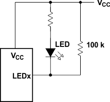
When the I/Os are used to control LEDs, normally they are connected to VCC through a resistor as shown in #SCPS126IMG2151. For a P-port configured as an input, ICC increases as VI becomes lower than VCC. The LED is a diode, with threshold voltage VT, and when a P-port is configured as an input the LED will be off but VI is a VT drop below VCC.
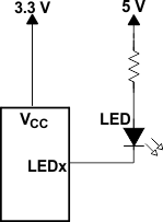
For battery-powered applications, it is essential that the voltage of P-ports controlling LEDs is greater than or equal to VCC when the P-ports are configured as input to minimize current consumption. #SCPS126IMG2151 shows a high-value resistor in parallel with the LED. #SCPS126IMG6593 shows VCC less than the LED supply voltage by at least VT. Both of these methods maintain the I/O VI at or above VCC and prevents additional supply current consumption when the P-port is configured as an input and the LED is off.
 Figure 9-2 High-Value Resistor in Parallel With LED
 Figure 9-3 Device Supplied by a Lower Voltage