JAJSFR3G October 2010 – November 2018 TCA9406
PRODUCTION DATA.
- 1 特長
- 2 アプリケーション
- 3 概要
- 4 改訂履歴
- 5 Pin Configuration and Functions
-
6 Specifications
- 6.1 Absolute Maximum Ratings
- 6.2 ESD Ratings
- 6.3 Recommended Operating Conditions
- 6.4 Thermal Information
- 6.5 Electrical Characteristics
- 6.6 Timing Requirements (VCCA = 1.8 V ± 0.15 V)
- 6.7 Timing Requirements (VCCA = 2.5 V ± 0.2 V)
- 6.8 Timing Requirements (VCCA = 3.3 V ± 0.3 V)
- 6.9 Switching Characteristics (VCCA = 1.8 V ± 0.15 V)
- 6.10 Switching Characteristics (VCCA = 2.5 V ± 0.2 V)
- 6.11 Switching Characteristics (VCCA = 3.3 V ± 0.3 V)
- 6.12 Typical Characteristics
- 7 Parameter Measurement Information
- 8 Detailed Description
- 9 Application and Implementation
- 10Power Supply Recommendations
- 11Layout
- 12デバイスおよびドキュメントのサポート
- 13メカニカル、パッケージ、および注文情報
パッケージ・オプション
メカニカル・データ(パッケージ|ピン)
サーマルパッド・メカニカル・データ
発注情報
8.3.1 Architecture
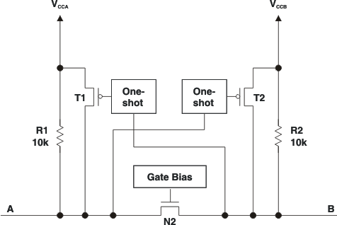
The TCA9406 architecture (see ) is an auto-direction-sensing based translator that does not require a direction-control signal to control the direction of data flow from A to B or from B to A.
 Figure 10. Architecture of a TCA9406 Cell
 These two bidirectional channels independently determine the direction of data flow without a direction-control signal. Each I/O pin is automatically reconfigured as either an input or an output, which is how this auto-direction feature is realized.
The TCA9406 is part of TI's "Switch" type voltage translator family and employs two key circuits to enable this voltage translation:
1) An N-channel pass-gate transistor topology that ties the A-port to the B-port
and
2) Output one-shot (O.S.) edge-rate accelerator circuitry to detect and accelerate rising edges on the A or B ports
For bidirectional voltage translation, pullup resistors are included on the device for dc current sourcing capability. The VGATE gate bias of the N-channel pass transistor is set at approximately one threshold voltage (VT) above the VCC level of the low-voltage side. Data can flow in either direction without guidance from a control signal.
The O.S. rising-edge rate accelerator circuitry speeds up the output slew rate by monitoring the input edge for transitions, helping maintain the data rate through the device. During a low-to-high signal rising edge, the O.S. circuits turn on the PMOS transistors (T1, T2) to increase the current drive capability of the driver for approximately 30 ns or 95% of the input edge, whichever occurs first. This edge-rate acceleration provides high ac drive by bypassing the internal 10-kΩ pullup resistors during the low-to-high transition to speed up the signal. The output resistance of the driver is decreased to approximately 50 Ω to 70 Ω during this acceleration phase. To minimize dynamic ICC and the possibility of signal contention, the user should wait for the O.S. circuit to turn off before applying a signal in the opposite direction. The worst-case duration is equal to the minimum pulse-width number provided in the Timing Requirements section of this data sheet.