SCPS199D August 2014 – October 2016 TCA9538
PRODUCTION DATA.
- 1 Features
- 2 Applications
- 3 Description
- 4 Revision History
- 5 Pin Configuration and Functions
- 6 Specifications
- 7 Parameter Measurement Information
- 8 Detailed Description
- 9 Application and Implementation
- 10Power Supply Recommendations
- 11Layout
- 12Device and Documentation Support
- 13Mechanical, Packaging, and Orderable Information
パッケージ・オプション
メカニカル・データ(パッケージ|ピン)
サーマルパッド・メカニカル・データ
発注情報
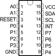
5 Pin Configuration and Functions
PW, DB Package
16-Pin TSSOP, SSOP
Top View

Pin Functions
| PIN | I/O | DESCRIPTION | |
|---|---|---|---|
| NAME | NO. | ||
| A0 | 1 | I | Address input. Connect directly to VCC or ground |
| A1 | 2 | I | Address input. Connect directly to VCC or ground |
| GND | 8 | — | Ground |
| INT | 13 | O | Interrupt output. Connect to VCC through a pull-up resistor |
| P0 | 4 | I/O | P-port input-output. Push-pull design structure. At power on, P0 is configured as an input |
| P1 | 5 | I/O | P-port input-output. Push-pull design structure. At power on, P1 is configured as an input |
| P2 | 6 | I/O | P-port input-output. Push-pull design structure. At power on, P2 is configured as an input |
| P3 | 7 | I/O | P-port input-output. Push-pull design structure. At power on, P3 is configured as an input |
| P4 | 9 | I/O | P-port input-output. Push-pull design structure. At power on, P4 is configured as an input |
| P5 | 10 | I/O | P-port input-output. Push-pull design structure. At power on, P5 is configured as an input |
| P6 | 11 | I/O | P-port input-output. Push-pull design structure. At power on, P6 is configured as an input |
| P7 | 12 | I/O | P-port input-output. Push-pull design structure. At power on, P7 is configured as an input |
| RESET | 3 | I | Active-low reset input. Connect to VCC through a pull-up resistor if no active connection is used |
| SCL | 14 | I | Serial clock bus. Connect to VCC through a pull-up resistor |
| SDA | 15 | I/O | Serial data bus. Connect to VCC through a pull-up resistor |
| VCC | 16 | — | Supply voltage |