JAJSH54E July   2009  – April 2019 TCA9555

PRODUCTION DATA.  

  1. 特長
  2. アプリケーション
  3. 概要
    1.     Device Images
      1.      概略回路図
  4. 改訂履歴
  5. 概要(続き)
  6. Pin Configuration and Functions
    1.     Pin Functions
  7. Specifications
    1. 7.1 Absolute Maximum Ratings
    2. 7.2 ESD Ratings
    3. 7.3 Recommended Operating Conditions
    4. 7.4 Thermal Information
    5. 7.5 Electrical Characteristics
    6. 7.6 I2C Interface Timing Requirements
    7. 7.7 Switching Characteristics
    8. 7.8 Typical Characteristics
  8. Parameter Measurement Information
  9. Detailed Description
    1. 9.1 Overview
    2. 9.2 Functional Block Diagram
    3. 9.3 Feature Description
      1. 9.3.1 5-V Tolerant I/O Ports
      2. 9.3.2 Hardware Address Pins
      3. 9.3.3 Interrupt (INT) Output
    4. 9.4 Device Functional Modes
      1. 9.4.1 Power-On Reset (POR)
      2. 9.4.2 Powered-Up
    5. 9.5 Programming
      1. 9.5.1 I/O Port
      2. 9.5.2 I2C Interface
        1. 9.5.2.1 Bus Transactions
          1. 9.5.2.1.1 Writes
          2. 9.5.2.1.2 Reads
      3. 9.5.3 Device Address
      4. 9.5.4 Control Register and Command Byte
    6. 9.6 Register Maps
      1. 9.6.1 Register Descriptions
  10. 10Application and Implementation
    1. 10.1 Application Information
    2. 10.2 Typical Application
      1. 10.2.1 Design Requirements
      2. 10.2.2 Detailed Design Procedure
        1. 10.2.2.1 Calculating Junction Temperature and Power Dissipation
        2. 10.2.2.2 Minimizing ICC When I/O Is Used to Control LED
        3. 10.2.2.3 Pull-Up Resistor Calculation
      3. 10.2.3 Application Curves
  11. 11Power Supply Recommendations
  12. 12Layout
    1. 12.1 Layout Guidelines
    2. 12.2 Layout Example
  13. 13デバイスおよびドキュメントのサポート
    1. 13.1 ドキュメントのサポート
      1. 13.1.1 関連資料
    2. 13.2 ドキュメントの更新通知を受け取る方法
    3. 13.3 コミュニティ・リソース
    4. 13.4 商標
    5. 13.5 静電気放電に関する注意事項
    6. 13.6 Glossary
  14. 14メカニカル、パッケージ、および注文情報

パッケージ・オプション

メカニカル・データ(パッケージ|ピン)
サーマルパッド・メカニカル・データ
発注情報

Writes

To write on the I2C bus, the master sends a START condition on the bus with the address of the slave, as well as the last bit (the R/W bit) set to 0, which signifies a write. After the slave sends the acknowledge bit, the master then sends the register address of the register to which it wishes to write. The slave acknowledges again, letting the master know it is ready. After this, the master starts sending the register data to the slave until the master has sent all the data necessary (which is sometimes only a single byte), and the master terminates the transmission with a STOP condition.

See the Control Register and Command Byte section to see list of the TCA9555's internal registers and a description of each one.

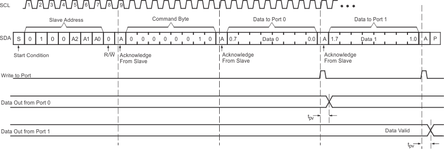
Figure 26 to Figure 28 show examples of writing a single byte to a slave register.
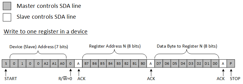
TCA9555 i2c_write.gifFigure 26. Write to Register

<br/>

TCA9555 i2c_example.gifFigure 27. Write to the Polarity Inversion Register
TCA9555 wr_out_cps200.gifFigure 28. Write to Output Port Registers