JAJSI95 December 2019 TL16C750E
PRODUCTION DATA.
- 1 特長
- 2 アプリケーション
- 3 概要
- 4 改訂履歴
- 5 概要 (続き)
- 6 Pin Configuration and Functions
- 7 Specifications
- 8 Parameter Measurement Information
-
9 Detailed Description
- 9.1 Overview
- 9.2 Functional Block Diagrams
- 9.3
Feature Description
- 9.3.1 UART Modes
- 9.3.2 Trigger Levels
- 9.3.3 Hardware Flow Control
- 9.3.4 Auto-RTS
- 9.3.5 Auto-CTS
- 9.3.6 Software Flow Control
- 9.3.7 Software Flow Control Example
- 9.3.8 Reset
- 9.3.9 Interrupts
- 9.3.10 Interrupt Mode Operation
- 9.3.11 Polled Mode Operation
- 9.3.12 Break and Timeout Conditions
- 9.3.13 Programmable Baud Rate Generator with Fractional Divisor
- 9.3.14 Fractional Divisor
- 9.4 Device Functional Modes
- 9.5
Register Maps
- 9.5.1 Registers Operations
- 9.5.2 Receiver Holding Register (RHR)
- 9.5.3 Transmit Holding Register (THR)
- 9.5.4 FIFO Control Register (FCR)
- 9.5.5 Line Control Register (LCR)
- 9.5.6 Line Status Register (LSR)
- 9.5.7 Modem Control Register (MCR)
- 9.5.8 Modem Status Register (MSR)
- 9.5.9 Interrupt Enable Register (IER)
- 9.5.10 Interrupt Identification Register (IIR)
- 9.5.11 Enhanced Feature Register (EFR)
- 9.5.12 Divisor Latches (DLL, DLH, DLF)
- 9.5.13 Transmission Control Register (TCR)
- 9.5.14 Trigger Level Register (TLR)
- 9.5.15 FIFO Ready Register
- 9.5.16 Alternate Function Register (AFR)
- 9.5.17 RS-485 Mode
- 9.5.18 IrDA Overview
- 9.5.19 IrDA Encoder Function
- 10Application and Implementation
- 11Power Supply Recommendations
- 12Layout
- 13デバイスおよびドキュメントのサポート
- 14メカニカル、パッケージ、および注文情報
パッケージ・オプション
メカニカル・データ(パッケージ|ピン)
- PFB|48
サーマルパッド・メカニカル・データ
- PFB|48
発注情報
9.3.13 Programmable Baud Rate Generator with Fractional Divisor
The TL16C750E UART contains a programmable baud generator that divides reference clock by a divisor in the range between 1 and (216 − 1) and a decimal resolution of 1/64. The output frequency of the baud rate generator is 8× or 16× the baud rate, depending on the value of DLF[7]. An additional divide-by-4 prescaler is also available and can be selected by MCR[7] as shown in the following. The formula for the divisor is:
Where 'baud divider' is either 8 or 16, depending on the value of DLF[7]. By default, DLF[7] = 0, which corresponds to a baud divider of 16 and

Figure 26 shows the internal prescaler and baud rate generator circuitry.
 Figure 26. Prescaler and Baud Rate Generator Block Diagram
 DLL and DLH must be written to in order to program the baud rate. DLL and DLH are the least significant and most significant byte of the baud rate divisor. If DLL and DLH are both 0, the UART is effectively disabled, because no baud clock is generated. The programmable baud rate generator is provided to select both the transmit and receive clock rates. Table 10 and Table 11 show the baud rate and divisor correlation for the crystal with frequency 1.8432 and 3.072 MHz, respectively.
Table 10. Baud Rates Using a 1.8432-MHz Crystal
| DESIRED BAUD RATE | DIVISOR USED TO GENERATE 16× CLOCK | PERCENT ERROR DIFFERENCE BETWEEN DESIRED AND ACTUAL |
|---|---|---|
| 50 | 2304 | 0 |
| 75 | 1536 | 0 |
| 110 | 1047 | 0.026 |
| 134.5 | 857 | 0.058 |
| 150 | 768 | 0 |
| 300 | 384 | 0 |
| 600 | 192 | 0 |
| 1200 | 96 | 0 |
| 1800 | 64 | 0 |
| 2000 | 58 | 0.69 |
| 2400 | 48 | 0 |
| 3600 | 32 | 0 |
| 4800 | 24 | 0 |
| 7200 | 16 | 0 |
| 9600 | 12 | 0 |
| 19200 | 6 | 0 |
| 38400 | 3 | 0 |
| 56000 | 2 | 2.86 |
Table 11. Baud Rates Using a 3.072-MHz Crystal
| DESIRED BAUD RATE | DIVISOR USED TO GENERATE 16× CLOCK | PERCENT ERROR DIFFERENCE BETWEEN DESIRED AND ACTUAL |
|---|---|---|
| 50 | 3840 | 0 |
| 75 | 2560 | 0 |
| 110 | 1745 | 0.026 |
| 134.5 | 1428 | 0.034 |
| 150 | 1280 | 0 |
| 300 | 640 | 0 |
| 600 | 320 | 0 |
| 1200 | 160 | 0 |
| 1800 | 107 | 0.312 |
| 2000 | 96 | 0 |
| 2400 | 80 | 0 |
| 3600 | 53 | 0.628 |
| 4800 | 40 | 0 |
| 7200 | 27 | 1.23 |
| 9600 | 20 | 0 |
| 19200 | 10 | 0 |
| 38400 | 5 | 0 |
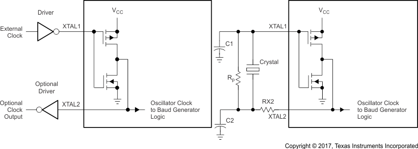
Figure 27 shows the crystal clock circuit reference.
