JAJSOU5D January   2006  – June 2022

PRODUCTION DATA  

  1. 特長
  2. アプリケーション
  3. 概要
  4. Revision History
  5. Pin Configuration and Functions
  6. Specifications
    1. 6.1 Absolute Maximum Ratings
    2. 6.2 ESD Ratings
    3. 6.3 Recommended Operating Conditions
    4. 6.4 Thermal Information
    5. 6.5 Electrical Characteristics — TL2575
    6. 6.6 Electrical Characteristics — TL2575HV
    7. 6.7 Typical Characteristics
  7. Parameter Measurement Information
    1. 7.1 Test Circuits
  8. Detailed Description
    1. 8.1 Overview
    2. 8.2 Functional Block Diagram
    3. 8.3 Feature Description
      1. 8.3.1 Feedback Connection
      2. 8.3.2 ON/OFF Input
    4. 8.4 Device Functional Modes
      1. 8.4.1 Standby Mode
  9. Application and Implementation
    1. 9.1 Typical Application
      1. 9.1.1 Design Requirements
      2. 9.1.2 Detailed Design Procedure
        1. 9.1.2.1 Input Capacitor (CIN)
        2. 9.1.2.2 Output Capacitor (COUT)
        3. 9.1.2.3 Catch Diode
        4. 9.1.2.4 Inductor
        5. 9.1.2.5 Output Voltage Ripple and Transients
        6. 9.1.2.6 Grounding
        7. 9.1.2.7 Reverse Current Considerations
        8. 9.1.2.8 Buck Regulator Design Procedure
        9. 9.1.2.9 Inductor Selection Guide
      3. 9.1.3 Application Curves
  10. 10Power Supply Recommendations
  11. 11Layout
    1. 11.1 Layout Guidelines
    2. 11.2 Layout Example
  12. 12Device and Documentation Support
    1. 12.1 Receiving Notification of Documentation Updates
    2. 12.2 サポート・リソース
    3. 12.3 Trademarks
    4. 12.4 静電気放電に関する注意事項
    5. 12.5 用語集
  13. 13Mechanical, Packaging, and Orderable Information
    1. 13.1 Package Option Addendum

パッケージ・オプション

メカニカル・データ(パッケージ|ピン)
サーマルパッド・メカニカル・データ
発注情報

Functional Block Diagram

GUID-E62F7AB8-2F64-45F5-91B0-9447BD0E8BDF-low.gif
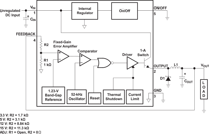
Pin numbers are for the KTT (TO-263) package.