SLVS028K April 1983 – September 2016 TL7702A , TL7705A , TL7709A , TL7712A , TL7715A
PRODUCTION DATA.
- 1 Features
- 2 Applications
- 3 Description
- 4 Revision History
- 5 Pin Configuration and Functions
- 6 Specifications
- 7 Parameter Measurement Information
- 8 Detailed Description
- 9 Application and Implementation
- 10Power Supply Recommendations
- 11Layout
- 12Device and Documentation Support
- 13Mechanical, Packaging, and Orderable Information
パッケージ・オプション
デバイスごとのパッケージ図は、PDF版データシートをご参照ください。
メカニカル・データ(パッケージ|ピン)
- D|8
- P|8
サーマルパッド・メカニカル・データ
発注情報
9 Application and Implementation
NOTE
Information in the following applications sections is not part of the TI component specification, and TI does not warrant its accuracy or completeness. TI’s customers are responsible for determining suitability of components for their purposes. Customers should validate and test their design implementation to confirm system functionality.
9.1 Application Information
This application shows the initialization circuit diagrams for a microprocessor system with supply voltage Vcc = 5 V. The external components required are the decoupling capacitor Cref for the reference voltage and the timing capacitor CT. The outputs of the TL77xxA are open collector outputs. In Figure 8 therefore a pull-up resistor is shown at the RESET output to ensure the correct HIGH level.
9.2 Typical Application
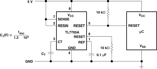 Figure 8. Reset Controller Schematic for a Microprocessor
9.2.1 Design Requirements
- 5-V microprocessor supply voltage
- td = 1.3 ms
9.2.2 Detailed Design Procedure
- Select reasonable values for pull-up/pull-down resistors for RESET and RESET. This design uses 10 kΩ.
- Choose CT = 0.1 µF to achieve td = 1.3 ms
- This design uses only the active-low reset output (RESET) because the example microcontroller resets when the input is Low.
9.2.3 Application Curves
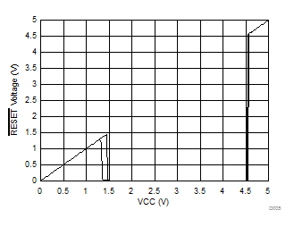 Figure 9. Supervisor RESET Output Voltage vs VCC
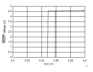 Figure 11. Supervisor RESET Output Voltage vs VCC at Transition
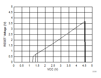 Figure 10. Supervisor RESET Output Voltage vs VCC
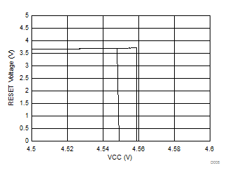 Figure 12. Supervisor RESET Output Voltage vs VCC at Transition
9.3 System Examples
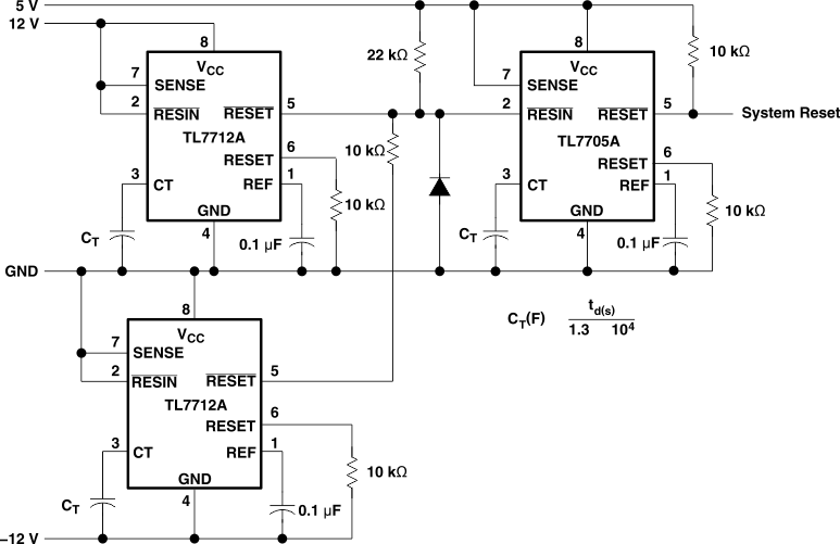 Figure 13. Multi Power-Supply System Reset Generation Schematic
 Figure 14. Eliminating Undefined States Using a P-Channel JFET Schematic
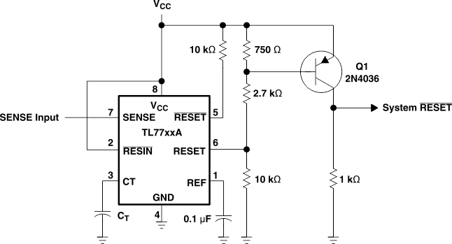 Figure 15. Eliminating Undefined States Using PNP Transistor Schematic