JAJSKL2O September   1989  – December 2020 TL7702B , TL7705B , TL7733B

PRODUCTION DATA  

  1. 特長
  2. アプリケーション
  3. 概要
  4. Revision History
  5. Pin Configuration and Functions
    1.     Pin Functions
  6. Specifications
    1. 6.1 Absolute Maximum Ratings
    2. 6.2 ESD Ratings
    3. 6.3 Recommended Operating Conditions
    4. 6.4 Thermal Information
    5. 6.5 Electrical Characteristics: TL77xxBC, TL77xxBI, and TL7705BQ
    6. 6.6 Switching Characteristics: TL77xxBC, TL77xxBI, and TL7705BQ
    7. 6.7 Timing Diagrams
    8. 6.8 Typical Characteristics
  7. Parameter Measurement Information
  8. Detailed Description
    1. 8.1 Overview
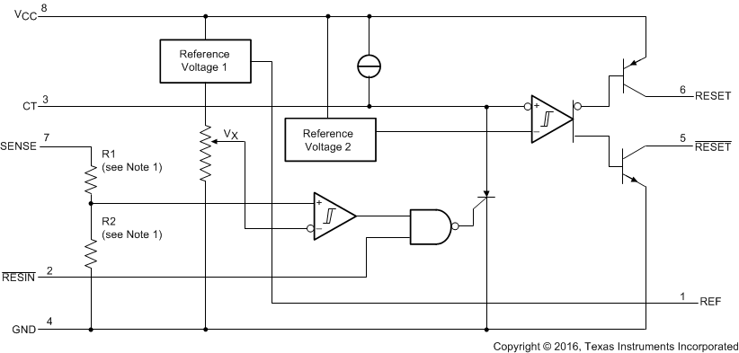
    2. 8.2 Functional Block Diagram
    3. 8.3 Feature Description
      1. 8.3.1 Wide Supply-Voltage Range
      2. 8.3.2 Adjustable Pulse Duration
    4. 8.4 Device Functional Modes
  9. Application and Implementation
    1. 9.1 Application Information
    2. 9.2 Typical Application
      1. 9.2.1 Design Requirements
      2. 9.2.2 Detailed Design Procedure
      3. 9.2.3 Application Curve
  10. 10Power Supply Recommendations
  11. 11Layout
    1. 11.1 Layout Guidelines
    2. 11.2 Layout Example
  12. 12Device and Documentation Support
    1. 12.1 Related Links
    2. 12.2 ドキュメントの更新通知を受け取る方法
    3. 12.3 サポート・リソース
    4. 12.4 Trademarks
    5. 12.5 静電気放電に関する注意事項
    6. 12.6 用語集
  13. 13Mechanical, Packaging, and Orderable Information

パッケージ・オプション

デバイスごとのパッケージ図は、PDF版データシートをご参照ください。

メカニカル・データ(パッケージ|ピン)
  • D|8
  • P|8
サーマルパッド・メカニカル・データ
発注情報

Functional Block Diagram

The functional block diagram is shown for illustrative purposes only; the actual circuit includes a trimming network to adjust the reference voltage and sense-comparator trip point.

GUID-09C5FAE0-FD07-476B-869F-B9488AED3D31-low.gif