SLOS467H October 2006 – January 2015 TL971 , TL972 , TL974
PRODUCTION DATA.
- 1 Features
- 2 Applications
- 3 Description
- 4 Simplified Schematic
- 5 Revision History
- 6 Pin Configuration and Functions
- 7 Specifications
- 8 Detailed Description
- 9 Application and Implementation
- 10Power Supply Recommendations
- 11Layout
- 12Device and Documentation Support
- 13Mechanical, Packaging, and Orderable Information
パッケージ・オプション
デバイスごとのパッケージ図は、PDF版データシートをご参照ください。
メカニカル・データ(パッケージ|ピン)
- D|8
- P|8
- DGK|8
- PW|8
サーマルパッド・メカニカル・データ
発注情報
7 Specifications
7.1 Absolute Maximum Ratings
over operating free-air temperature range (unless otherwise noted)(1)| MIN | MAX | UNIT | |||
|---|---|---|---|---|---|
| VCC | Supply voltage range | 2.7 | 15 | V | |
| VID | Differential input voltage(2) | ±1 V | V | ||
| VIN | Input voltage range(3) | VCC– – 0.3 | VCC+ + 0.3 | V | |
| TJ | Maximum junction temperature | 150 | °C | ||
| Tstg | Storage temperature range | –65 | 150 | °C | |
(1) Stresses beyond those listed under Absolute Maximum Ratings may cause permanent damage to the device. These are stress ratings only, and functional operation of the device at these or any other conditions beyond those indicated under Recommended Operating Conditionsis not implied. Exposure to absolute-maximum-rated conditions for extended periods may affect device reliability.
(2) Differential voltages for the noninverting input terminal are with respect to the inverting input terminal.
(3) The input and output voltages must never exceed VCC + 0.3 V.
7.2 ESD Ratings
| VALUE | UNIT | |||
|---|---|---|---|---|
| V(ESD) | Electrostatic discharge | Human body model (HBM), per ANSI/ESDA/JEDEC JS-001, all pins(1) | 2000 | V |
| Charged device model (CDM), per JEDEC specification JESD22-C101, all pins(2) | 1500 | |||
(1) JEDEC document JEP155 states that 500-V HBM allows safe manufacturing with a standard ESD control process.
(2) JEDEC document JEP157 states that 250-V CDM allows safe manufacturing with a standard ESD control process.
7.3 Recommended Operating Conditions
| MIN | MAX | UNIT | ||
|---|---|---|---|---|
| VCC | Supply voltage | 2.7 | 12 | V |
| VICM | Common-mode input voltage | VCC– + 1.15 | VCC+ – 1.15 | V |
| TA | Operating free-air temperature | –40 | 125 | °C |
7.4 Thermal Information
| THERMAL METRIC(1) | TL971 | TL972 | TL974 | UNIT | ||||||||
|---|---|---|---|---|---|---|---|---|---|---|---|---|
| D(2) | DBV(2) | D(2) | DGK(3) | DRG(3) | P(2) | PW(2) | D(2) | N(2) | PW(2) | |||
| 8 PINS | 5 PINS | 8 PINS | 14 PINS | |||||||||
| RθJA | Package thermal impedance, junction to free air | 97 | 206 | 97 | 172 | 44 | 85 | 149 | 86 | 80 | 113 | °C/W |
(1) For more information about traditional and new thermal metrics, see the IC Package Thermal Metrics application report (SPRA953).
(2) Package thermal impedance is calculated in accordance with JESD 51-7.
(3) Package thermal impedance is calculated in accordance with JESD 51-5.
7.5 Electrical Characteristics
VCC+ = 2.5 V, VCC– = –2.5 V, full-range TA = –40°C to 125°C (unless otherwise noted)7.6 Typical Characteristics
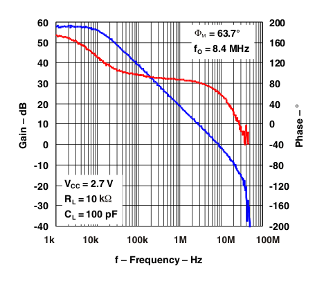 Figure 1. Gain And Phase vs Frequency
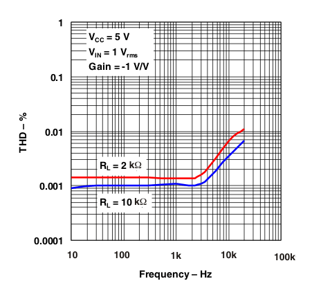 Figure 3. Total Harmonic Distortion vs Frequency
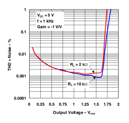 Figure 5. Total Harmonic Distortion + Noise vs Output Voltage
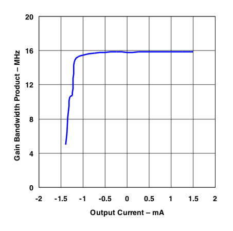 Figure 7. Gain Bandwidth Product vs Output Current
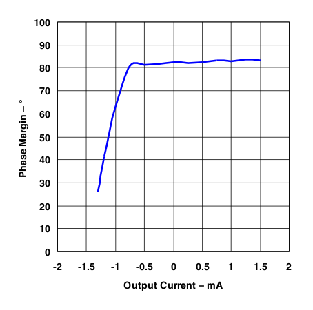 Figure 9. Phase Margin vs Output Current
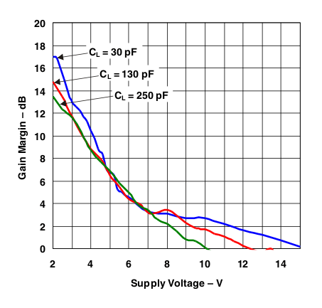 Figure 11. Gain Margin vs Supply Voltage
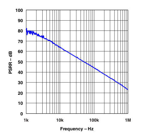 Figure 13. Power-Supply Ripple Rejection vs Frequency
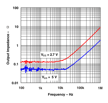 Figure 15. Output Impedance vs Frequency
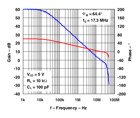 Figure 2. Gain And Phase vs Frequency
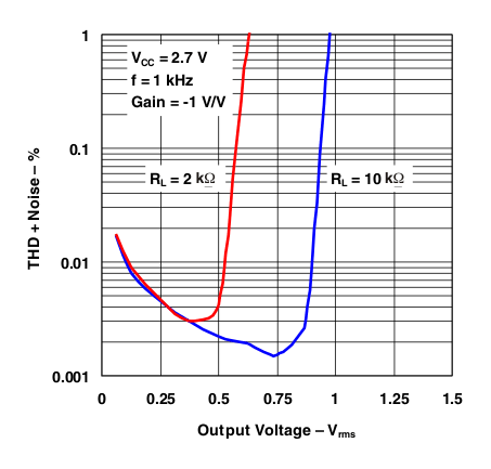 Figure 4. Total Harmonic Distortion + Noise vs Output Voltage
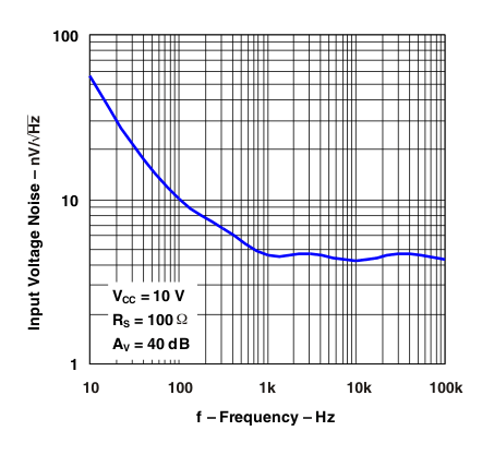 Figure 6. Input Voltage Noise vs Frequency
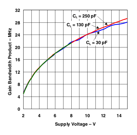 Figure 8. Gain Bandwidth Product vs Supply Voltage
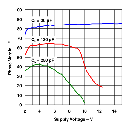 Figure 10. Phase Margin vs Supply Voltage
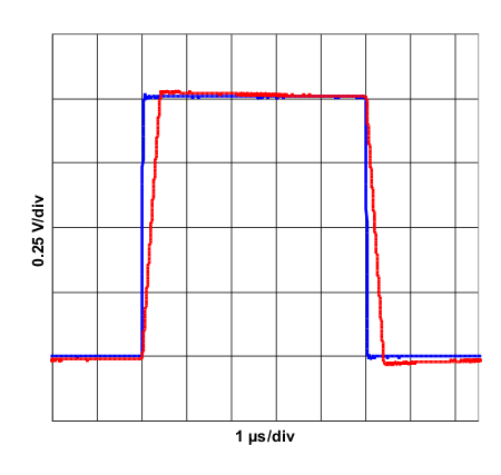 Figure 12. Input Response
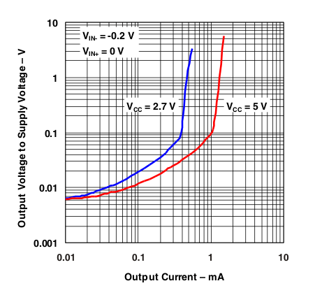 Figure 14. Output Voltage vs Output Current
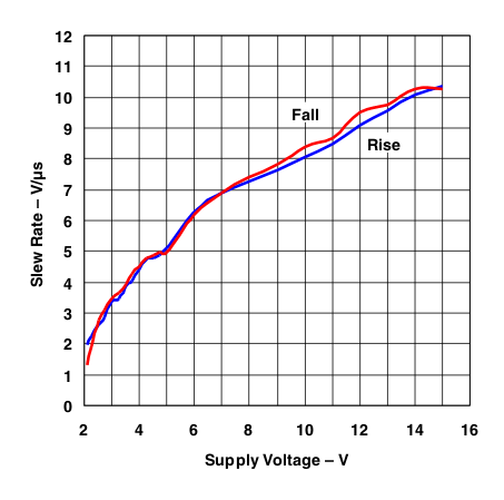 Figure 16. Slew Rate vs Supply Voltage