JAJSE50 November   2017 TLA2021 , TLA2022 , TLA2024

PRODUCTION DATA.  

  1. 特長
  2. アプリケーション
  3. 概要
    1.     Device Images
      1.      システム監視アプリケーションの例
  4. 改訂履歴
  5. 概要(続き)
  6. Device Comparison Table
  7. Pin Configuration and Functions
    1.     Pin Functions
  8. Specifications
    1. 8.1 Absolute Maximum Ratings
    2. 8.2 ESD Ratings
    3. 8.3 Recommended Operating Conditions
    4. 8.4 Thermal Information
    5. 8.5 Electrical Characteristics
    6. 8.6 I2C Timing Requirements
    7. 8.7 Typical Characteristics
  9. Detailed Description
    1. 9.1 Overview
    2. 9.2 Functional Block Diagrams
    3. 9.3 Feature Description
      1. 9.3.1 Multiplexer
      2. 9.3.2 Analog Inputs
      3. 9.3.3 Full-Scale Range (FSR) and LSB Size
      4. 9.3.4 Voltage Reference
      5. 9.3.5 Oscillator
      6. 9.3.6 Output Data Rate and Conversion Time
    4. 9.4 Device Functional Modes
      1. 9.4.1 Reset and Power-Up
      2. 9.4.2 Operating Modes
        1. 9.4.2.1 Single-Shot Conversion Mode
        2. 9.4.2.2 Continuous-Conversion Mode
    5. 9.5 Programming
      1. 9.5.1 I2C Interface
        1. 9.5.1.1 I2C Address Selection
        2. 9.5.1.2 I2C Interface Speed
        3. 9.5.1.3 Serial Clock (SCL) and Serial Data (SDA)
        4. 9.5.1.4 I2C Data Transfer Protocol
        5. 9.5.1.5 Timeout
        6. 9.5.1.6 I2C General-Call (Software Reset)
      2. 9.5.2 Reading and Writing Register Data
        1. 9.5.2.1 Reading Conversion Data or the Configuration Register
        2. 9.5.2.2 Writing the Configuration Register
      3. 9.5.3 Data Format
  10. 10Register Maps
    1. 10.1 Conversion Data Register (RP = 00h) [reset = 0000h]
      1. Table 6. Conversion Data Register Field Descriptions
    2. 10.2 Configuration Register (RP = 01h) [reset = 8583h]
      1. Table 7. Configuration Register Field Descriptions
  11. 11Application and Implementation
    1. 11.1 Application Information
      1. 11.1.1 Basic Interface Connections
      2. 11.1.2 Connecting Multiple Devices
      3. 11.1.3 Single-Ended Signal Measurements
      4. 11.1.4 Analog Input Filtering
      5. 11.1.5 Duty Cycling To Reduce Power Consumption
      6. 11.1.6 I2C Communication Sequence Example
    2. 11.2 Typical Application
      1. 11.2.1 Design Requirements
      2. 11.2.2 Detailed Design Procedure
      3. 11.2.3 Application Curve
  12. 12Power Supply Recommendations
    1. 12.1 Power-Supply Sequencing
    2. 12.2 Power-Supply Decoupling
  13. 13Layout
    1. 13.1 Layout Guidelines
    2. 13.2 Layout Example
  14. 14デバイスおよびドキュメントのサポート
    1. 14.1 デバイス・サポート
      1. 14.1.1 デベロッパー・ネットワークの製品に関する免責事項
    2. 14.2 関連リンク
    3. 14.3 ドキュメントの更新通知を受け取る方法
    4. 14.4 コミュニティ・リソース
    5. 14.5 商標
    6. 14.6 静電気放電に関する注意事項
    7. 14.7 Glossary
  15. 15メカニカル、パッケージ、および注文情報

パッケージ・オプション

メカニカル・データ(パッケージ|ピン)
サーマルパッド・メカニカル・データ
発注情報

Basic Interface Connections

Figure 18 shows the principle I2C connections for the TLA202x.
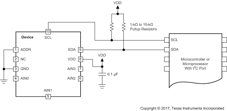
TLA2021 TLA2022 TLA2024 ai_basic_connection_bas822.gifFigure 18. Typical Interface Connections of the TLA202x

The TLA202x interface directly to standard-mode or fast-mode I2C controllers. Any microcontroller I2C peripheral, including master-only and single-master I2C peripherals, operates with the TLA202x. The TLA202x do not perform clock-stretching (that is, the devices never pull the clock line low), so this function does not need to be provided for unless other clock-stretching devices are present on the same I2C bus.

Pullup resistors are required on both the SDA and SCL lines because I2C bus drivers are open-drain. The size of these resistors depends on the bus operating speed and capacitance of the bus lines. Higher-value resistors yield lower power consumption when the bus lines are pulled low, but increase the transition times on the bus, which limits the bus speed. Lower-value resistors allow higher interface speeds, but at the expense of higher power consumption when the bus lines are pulled low. Long bus lines have higher capacitance and require smaller pullup resistors to compensate. Do not use resistors that are too small because the bus drivers may be unable to pull the bus lines low.

See the I2C-Bus Specification and User Manual from NXP Semiconductors for more details on pullup resistor sizing.