JAJSHO0J August 1983 – November 2023 TLC555
PRODUCTION DATA
- 1
- 1 特長
- 2 アプリケーション
- 3 概要
- 4 Pin Configuration and Functions
-
5 Specifications
- 5.1 Absolute Maximum Ratings
- 5.2 ESD Ratings
- 5.3 Recommended Operating Conditions
- 5.4 Thermal Information
- 5.5 Electrical Characteristics: VDD = 2 V for TLC555C, VDD = 3 V for TLC555I
- 5.6 Electrical Characteristics: VDD = 5 V
- 5.7 Electrical Characteristics: VDD = 15 V
- 5.8 Timing Characteristics
- 5.9 Typical Characteristics
- 6 Detailed Description
- 7 Application and Implementation
- 8 Device and Documentation Support
- 9 Revision History
- 10Mechanical, Packaging, and Orderable Information
パッケージ・オプション
メカニカル・データ(パッケージ|ピン)
サーマルパッド・メカニカル・データ
発注情報
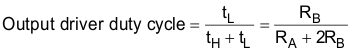
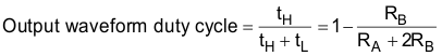
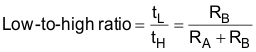
6.3.2 Astable Operation
As shown in Figure 6-5, adding a second resistor, RB, to the circuit of Figure 6-2 and connecting the trigger input to the threshold input causes the timer to self-trigger and run as a multivibrator. The capacitor C charges through RA and RB and then discharges through RB only. Therefore, the duty cycle is controlled by the values of RA and RB.
This astable connection results in
capacitor C charging and discharging between the threshold-voltage level
(≈ 0.67 × VCC) and the trigger-voltage
level (≈ 0.33 × VCC). As in the monostable circuit, charge and discharge
times (and, therefore, the frequency and duty cycle) are independent of the supply
voltage.

| Decouple CONT voltage to ground with a capacitor to improve operation. Reevaluate for individual applications. |

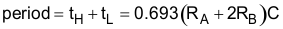
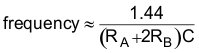
Figure 6-6 shows typical waveforms generated during astable operation. The output high-level duration tH and low-level duration tL for frequencies below 100 kHz can be calculated as follows:
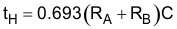
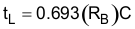
Other useful relationships are shown below:
Equation 1 to Equation 7 do not account for any propagation delay times from the TRIG and THRES inputs to DISCH output. These delay times add directly to the period and overcharge the capacitor, which creates differences between calculated and actual values that increase with frequency. In addition, the internal on-state resistance ron during discharge adds to RB to provide another source of timing error in the calculation when RB is very low. The following equations provide better agreement with measured values. The formulas in Equation 8 represent the actual low and high times when used at higher frequencies (beyond 100 kHz) because propagation delay and discharge on resistance is added to the formulas. The value of CT includes both the nominal or deliberate timing capacitance, as well as parasitic capacitance on the PCB. Decoupling capacitance on CONT also affects the duty cycle, with an error contribution that depends on the capacitor leakage resistance. For additional discussion, see the Design low-duty-cycle timer circuits article.
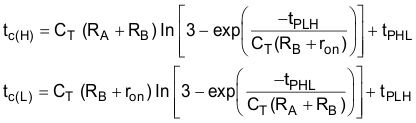
These equations and those given earlier are similar in that a time constant is multiplied by the logarithm of a number or function. The limit values of the logarithmic terms must be between ln(2) at low frequencies, and ln(3) at extremely high frequencies. For a duty cycle close to 50%, an appropriate constant for the logarithmic terms can be substituted with good results. Output waveform duty cycles less than 50% require that tc(H) / tc(L) < 1 and possibly that RA ≤ ron. These conditions can be difficult to obtain. Figure 6-8 shows the nominal free-running frequency associated with various combinations of CT and RA + 2 × RB.
 Figure 6-7 Trigger and Threshold Voltage Waveform
 Figure 6-8 Nominal Free-Running Frequency vs Timing Capacitance
Resistance = RA + 2 × RB