SLVS867B May 2009 – August 2015 TLC59213 , TLC59213A
PRODUCTION DATA.
- 1 Features
- 2 Applications
- 3 Description
- 4 Revision History
- 5 Pin Configuration and Functions
- 6 Specifications
- 7 Parameter Measurement Information
- 8 Detailed Description
- 9 Application and Implementation
- 10Power Supply Recommendations
- 11Layout
- 12Device and Documentation Support
- 13Mechanical, Packaging, and Orderable Information
パッケージ・オプション
メカニカル・データ(パッケージ|ピン)
サーマルパッド・メカニカル・データ
発注情報
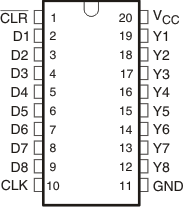
5 Pin Configuration and Functions
N or PW Package
20-Pin PDIP or TSSOP
Top View

Pin Functions
| PIN | I/O | DESCRIPTION | |
|---|---|---|---|
| NAME | NO. | ||
| CLR | 1 | I | Direct clear of output |
| D1 | 2 | I | Input control to the current source driver |
| D2 | 3 | I | Input control to the current source driver |
| D3 | 4 | I | Input control to the current source driver |
| D4 | 5 | I | Input control to the current source driver |
| D5 | 6 | I | Input control to the current source driver |
| D6 | 7 | I | Input control to the current source driver |
| D7 | 8 | I | Input control to the current source driver |
| D8 | 9 | I | Input control to the current source driver |
| CLK | 10 | I | Clock to positive edge triggered D flipflops |
| GND | 11 | — | Ground |
| Y8 | 12 | O | Output to load |
| Y7 | 13 | O | Output to load |
| Y6 | 14 | O | Output to load |
| Y5 | 15 | O | Output to load |
| Y4 | 16 | O | Output to load |
| Y3 | 17 | O | Output to load |
| Y2 | 18 | O | Output to load |
| Y1 | 19 | O | Output to load |
| Vcc | 20 | I | Supply voltage |