SLVSFI5A October   2020  – December 2020 TLC6C5748-Q1

PRODUCTION DATA  

  1. Features
  2. Applications
  3. Description
  4. Revision History
  5. Terminal Configurations and Functions
  6. Specifications
    1. 6.1 Absolute Maximum Ratings
    2. 6.2 ESD Ratings
    3. 6.3 Recommended Operating Conditions
    4. 6.4 Thermal Information
    5. 6.5 Electrical Characteristics
    6. 6.6 Switching Characteristics
    7. 6.7 Typical Characteristics
  7. Parameter Measurement Information
    1. 7.1 Terminal-Equivalent Input and Output Schematic Diagrams
    2. 7.2 Test Circuits
    3. 7.3 Timing Diagrams
  8. Detailed Description
    1. 8.1 Overview
    2. 8.2 Functional Block Diagram
    3. 8.3 Feature Description
      1. 8.3.1 Output Current Calculation
      2. 8.3.2 Register and Data Latch Configuration
        1. 8.3.2.1 769-Bit Common Shift Register
        2. 8.3.2.2 Grayscale (GS) Data Latch
        3. 8.3.2.3 Control Data Latch
        4. 8.3.2.4 Dot Correction (DC) Data Latch
        5. 8.3.2.5 Maximum Current (MC) Data Latch
        6. 8.3.2.6 Global Brightness Control (BC) Data Latch
        7. 8.3.2.7 Function Control (FC) Data Latch
      3. 8.3.3 Status Information Data (SID)
      4. 8.3.4 LED Open Detection (LOD)
      5. 8.3.5 LED Short Detection (LSD)
      6. 8.3.6 Thermal Shutdown Faults (TSD)
      7. 8.3.7 Noise Reduction
    4. 8.4 Device Functional Modes
      1. 8.4.1 Maximum Current Control (MC) Function
      2. 8.4.2 Dot Correction (DC) Function
      3. 8.4.3 Global Brightness Control (BC) Function
      4. 8.4.4 Grayscale (GS) Function (PWM Control)
        1. 8.4.4.1 Conventional PWM Control
        2. 8.4.4.2 Enhanced Spectrum (ES) PWM Control
        3. 8.4.4.3 Auto Display Repeat Function
        4. 8.4.4.4 Display Timing Reset Function
        5. 8.4.4.5 Auto Data Refresh Function
  9. Application and Implementation
    1. 9.1 Application Information
    2. 9.2 Typical Application
      1. 9.2.1 Daisy-Chain Application
        1. 9.2.1.1 Design Requirements
        2. 9.2.1.2 Detailed Design Procedure
          1. 9.2.1.2.1 Step-by-Step Design Procedure
          2. 9.2.1.2.2 Maximum Current (MC) Data
          3. 9.2.1.2.3 Global Brightness Control (BC) Data
          4. 9.2.1.2.4 Dot Correction (DC) Data
          5. 9.2.1.2.5 Grayscale (GS) Data
          6. 9.2.1.2.6 Other Control Data
        3. 9.2.1.3 Application Curves
  10. 10Power Supply Recommendations
  11. 11Layout
    1. 11.1 Layout Guidelines
    2. 11.2 Layout Example
  12. 12Device and Documentation Support
    1. 12.1 Receiving Notification of Documentation Updates
    2. 12.2 Support Resources
    3. 12.3 Trademarks
    4. 12.4 Electrostatic Discharge Caution
    5. 12.5 Glossary
  13. 13Mechanical, Packaging, and Orderable Information

パッケージ・オプション

メカニカル・データ(パッケージ|ピン)
サーマルパッド・メカニカル・データ
発注情報

Control Data Latch

The control data latch is 371 bits long. The data latch contains dot correction (DC) data, maximum current (MC) data, global brightness control (BC) data, and function control (FC) data. The DC for each constant-current output are controlled by the data in the DC data latch. The control data in the data latch are updated with the lower 371 bits of the common shift register at the LAT rising edge when the common shift register MSB is 1. The 336 bits of DC data are copied from the control data latch when the 65,536th GSCLK is input with RFRESH set to 1 in the control data latch after the GS data are written or the LAT rising edge for GS data writes is input when the RFRESH bit is 0.

When the device is powered up, the data in the control data latch (except the MC bits) are random. Therefore, DC, BC, and FC data must be written to the control data latch before turning on the constant-current outputs. Furthermore, MC data should be set appropriately for the application. Refer to Figure 8-3 for a control data write timing diagram.
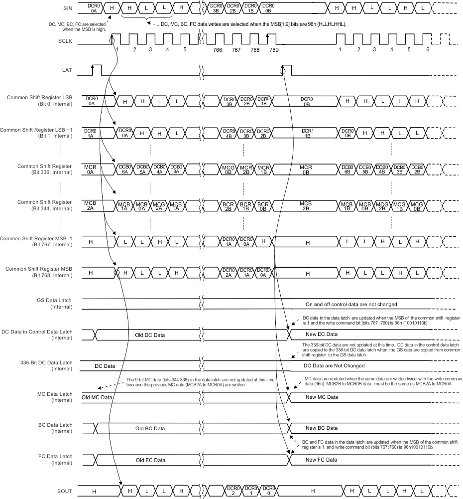
GUID-788E89B0-9FF0-43A5-B6F8-BC9BE539B848-low.gifFigure 8-3 Control Data Write Timing Diagram for DC, MC, BC, and FC