SLVS647I August 2006 – November 2014 TLE4275-Q1
UNLESS OTHERWISE NOTED, this document contains PRODUCTION DATA.
- 1 Features
- 2 Applications
- 3 Description
- 4 Revision History
- 5 Pin Configuration and Functions
- 6 Specifications
- 7 Parameter Measurement Information
- 8 Detailed Description
- 9 Application and Implementation
- 10Power Supply Recommendations
- 11Layout
- 12Device and Documentation Support
- 13Mechanical, Packaging, and Orderable Information
パッケージ・オプション
デバイスごとのパッケージ図は、PDF版データシートをご参照ください。
メカニカル・データ(パッケージ|ピン)
- KTT|5
- PWP|20
- KVU|5
サーマルパッド・メカニカル・データ
発注情報
9 Application and Implementation
NOTE
Information in the following applications sections is not part of the TI component specification, and TI does not warrant its accuracy or completeness. TI’s customers are responsible for determining suitability of components for their purposes. Customers should validate and test their design implementation to confirm system functionality.
9.1 Application Information
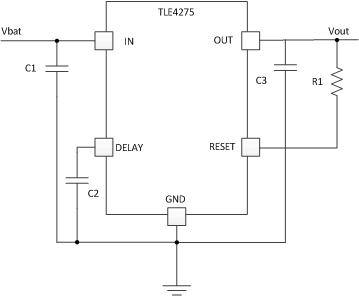
Figure 19 shows typical application circuits for the TLE4275-Q1. Based on the end-application, different values of external components can be used. An application can require a larger output capacitor during fast load steps in order to prevent a reset from occurring. TI recommends a low-ESR ceramic capacitor with a dielectric of type X5R or X7R for better load transient response.
9.2 Typical Application
 Figure 19. Typical Application Diagram
9.2.1 Design Requirements
For this design example, use the parameters listed in Table 1.
Table 1. Design Parameters
| DESIGN PARAMETER | EXAMPLE VALUE |
|---|---|
| Input voltage range | 4 to 40 V |
| Output voltage | 5 V |
| Output current rating | 400 mA |
| Output capacitor range | 10 to 500 µF |
| Output capacitor ESR range | 1 mΩ to 20 Ω |
| DELAY capacitor range | 100 pF to 500 nF |
9.2.2 Detailed Design Procedure
To begin the design process, determine the following:
- Input voltage range
- Output voltage
- Output current rating
- Output capacitor
- Power-up reset delay time
9.2.2.1 Power-Up Reset Capacitance
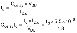
To calculate the power-up reset capacitance, use Equation 2.

9.2.2.2 Thermal Consideration
Calculate the power dissipated by the device according to Equation 3.
where
- PT = Total power dissipation of the device.
- IO = output current
- VI = input voltage
- VO = output voltage
After determining the power dissipated by the device, calculate the junction temperature from the ambient temperature and the device thermal impedance.
9.2.3 Application Curves
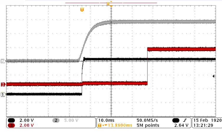
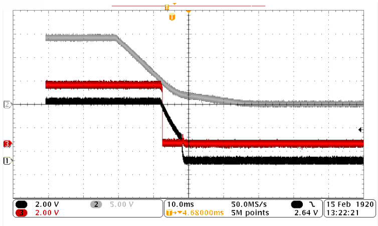
Load = 200 mA, Cin = 22 µF, Cout = 10 µF
