JAJSME2A december   2022  – august 2023 TLV1851 , TLV1861

PRODMIX  

  1.   1
  2. 特長
  3. アプリケーション
  4. 概要
  5. Revision History
  6. Pin Configuration and Functions
    1.     Pin Configuration: TLV1851 and TLV1861
    2.     Pin Configurations: TLV1852 and TLV1862
    3.     Pin Configurations: TLV1854 and TLV1864
  7. Specifications
    1. 6.1 Absolute Maximum Ratings
    2. 6.2 ESD Ratings
    3. 6.3 Thermal Information
    4. 6.4 Recommended Operating Conditions
    5. 6.5 Electrical Characteristics
    6. 6.6 Switching Characteristics
    7. 6.7 Typical Characteristics
  8. Detailed Description
    1. 7.1 Overview
    2. 7.2 Functional Block Diagrams
    3. 7.3 Feature Description
    4. 7.4 Device Functional Modes
      1. 7.4.1 Inputs
        1. 7.4.1.1 Operating Common-Mode Ranges
        2. 7.4.1.2 Fail-Safe Inputs
        3. 7.4.1.3 Unused Inputs
      2. 7.4.2 Internal Hysteresis
      3. 7.4.3 Outputs
        1. 7.4.3.1 TLV185x Push-Pull Output
        2. 7.4.3.2 TLV186x Open-Drain Output
      4. 7.4.4 ESD Protection
        1. 7.4.4.1 Inputs
        2. 7.4.4.2 Outputs
      5. 7.4.5 Power-On Reset (POR)
      6. 7.4.6 Reverse Battery Protection
  9. Application and Implementation
    1. 8.1 Application Information
      1. 8.1.1 Basic Comparator Definitions
        1. 8.1.1.1 Operation
        2. 8.1.1.2 Propagation Delay
        3. 8.1.1.3 Overdrive Voltage
      2. 8.1.2 Hysteresis
        1. 8.1.2.1 Inverting Comparator With Hysteresis
        2. 8.1.2.2 Non-Inverting Comparator With Hysteresis
        3. 8.1.2.3 Inverting and Non-Inverting Hysteresis using Open-Drain Output
    2. 8.2 Typical Applications
      1. 8.2.1 Window Comparator
        1. 8.2.1.1 Design Requirements
        2. 8.2.1.2 Detailed Design Procedure
        3. 8.2.1.3 Application Curve
      2. 8.2.2 Undervoltage Detection
      3. 8.2.3 Reverse Battery and Overvoltage Protection Scheme
    3. 8.3 Power Supply Recommendations
  10. Layout
    1. 9.1 Layout Guidelines
    2. 9.2 Layout Example
  11. 10デバイスおよびドキュメントのサポート
    1. 10.1 Documentation Support
      1. 10.1.1 Related Documentation
    2. 10.2 ドキュメントの更新通知を受け取る方法
    3. 10.3 サポート・リソース
    4. 10.4 Trademarks
    5. 10.5 静電気放電に関する注意事項
    6. 10.6 用語集
  12. 11Mechanical, Packaging, and Orderable Information

パッケージ・オプション

メカニカル・データ(パッケージ|ピン)
サーマルパッド・メカニカル・データ
発注情報

Non-Inverting Comparator With Hysteresis

A non-inverting comparator with hysteresis requires a two-resistor network and a voltage reference (VREF) at the inverting input, as shown in Figure 8-5,

GUID-84EAC0CF-F005-4725-9FED-A433B1B3B458-low.gifFigure 8-5 TLV185x in a Non-Inverting Configuration With Hysteresis

The equivalent resistor networks when the output is high and low are shown in Figure 8-6.

GUID-0896F943-F1F9-452F-94DB-837722BD7DEE-low.gifFigure 8-6 Non-Inverting Configuration Resistor Networks

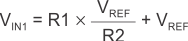
When VIN is less than VREF,, the output is low. For the output to switch from low to high, VIN must rise above the VIN1 threshold. Use Equation 4 to calculate VIN1.

Equation 4. GUID-1599C606-8F8B-4097-A385-FC7FB73DCCD1-low.gif

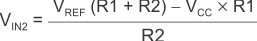
When VIN is greater than VREF, the output is high. For the comparator to switch back to a low state, VIN must drop below VIN2. Use Equation 5 to calculate VIN2.

Equation 5. GUID-636B3E40-CB3B-4092-A85E-A06AB89F611C-low.gif

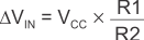
The hysteresis of this circuit is the difference between VIN1 and VIN2, as shown in Equation 6.

Equation 6. GUID-9160F8A9-AF09-4147-8CDB-7D9969E0FD70-low.gif

For more information, please see Application Notes SNOA997 "Inverting comparator with hysteresis circuit" and SBOA313 "Non-Inverting Comparator With Hysteresis Circuit".