SLOS922A September 2015 – December 2015 TLV27L2-Q1
PRODUCTION DATA.
- 1 Features
- 2 Applications
- 3 Description
- 4 Revision History
- 5 Selection Guide
- 6 Pin Configuration and Functions
- 7 Specifications
- 8 Detailed Description
- 9 Application and Implementation
- 10Power Supply Recommendations
- 11Layout
- 12Device and Documentation Support
- 13Mechanical, Packaging, and Orderable Information
8 Detailed Description
8.1 Overview
The TLV27L2-Q1 device is a micropower, rail-to-rail output, operational amplifier. This device operates from 2.7 V to 16 V, is unity-gain stable, and is suitable for a wide range of general-purpose applications. The class AB output stage is capable of driving ≤ 10-kΩ loads connected to any point between V+ and ground. The input common-mode voltage range includes the negative rail and allows the TLV27L2-Q1 device to be used in virtually any single-supply application from 2.7 V to 16 V. The typical supply current of 7 µA makes the TLV27L2-Q1 device an excellent choice for battery operated systems.
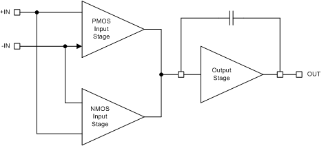
8.2 Functional Block Diagram

8.3 Feature Description
8.3.1 Offset Voltage
The output offset voltage (VOO) is the sum of the input offset voltage (VIO) and both input bias currents (IIB) times the corresponding gains. Use the schematic and formula in Figure 25 to calculate the output offset voltage.
 Figure 25. Output Offset Voltage Model
8.4 Device Functional Modes
The TLV27L2-Q1 device is powered on when the supply is connected. The device can be operated as a single-supply operational amplifier or a dual-supply amplifier, depending on the application. The TLV27L2-Q1 device operates from power supplies as low as 2.7 V or as high as 16 V.