JAJSL95G March   2007  – February 2021 TLV320AIC3104

PRODUCTION DATA  

  1. 特長
  2. アプリケーション
  3. 概要
  4. Revision History
  5. 概要 (続き)
  6. Device Comparison Table
  7. Pin Configuration and Functions
  8. Specifications
    1. 8.1 Absolute Maximum Ratings
    2. 8.2 ESD Ratings
    3. 8.3 Recommended Operating Conditions
    4. 8.4 Thermal Information
    5. 8.5 Electrical Characteristics
    6. 8.6 Audio Data Serial Interface Timing Requirements
    7. 8.7 Timing Diagrams
    8. 8.8 Typical Characteristics
  9. Parameter Measurement Information
  10. 10Detailed Description
    1. 10.1 Overview
    2. 10.2 Functional Block Diagrams
    3. 10.3 Feature Description
      1. 10.3.1  Hardware Reset
      2. 10.3.2  Digital Audio Data Serial Interface
        1. 10.3.2.1 Right-Justified Mode
        2. 10.3.2.2 Left-Justified Mode
        3. 10.3.2.3 I2S Mode
        4. 10.3.2.4 DSP Mode
        5. 10.3.2.5 TDM Data Transfer
      3. 10.3.3  Audio Data Converters
        1. 10.3.3.1 Audio Clock Generation
        2. 10.3.3.2 Stereo Audio ADC
          1. 10.3.3.2.1 Stereo Audio ADC High-Pass Filter
          2. 10.3.3.2.2 Automatic Gain Control (AGC)
            1. 10.3.3.2.2.1 Target Level
            2. 10.3.3.2.2.2 Attack Time
            3. 10.3.3.2.2.3 Decay Time
            4. 10.3.3.2.2.4 Noise Gate Threshold
            5. 10.3.3.2.2.5 Maximum PGA Gain Applicable
      4. 10.3.4  Stereo Audio DAC
        1. 10.3.4.1 Digital Audio Processing for Playback
        2. 10.3.4.2 Digital Interpolation Filter
        3. 10.3.4.3 Delta-Sigma Audio DAC
        4. 10.3.4.4 Audio DAC Digital Volume Control
        5. 10.3.4.5 Increasing DAC Dynamic Range
        6. 10.3.4.6 Analog Output Common-Mode Adjustment
        7. 10.3.4.7 Audio DAC Power Control
      5. 10.3.5  Audio Analog Inputs
      6. 10.3.6  Analog Fully Differential Line Output Drivers
      7. 10.3.7  Analog High-Power Output Drivers
      8. 10.3.8  Input Impedance and VCM Control
      9. 10.3.9  MICBIAS Generation
      10. 10.3.10 Short-Circuit Output Protection
      11. 10.3.11 Jack and Headset Detection
    4. 10.4 Device Functional Modes
      1. 10.4.1 Bypass Path Mode
        1. 10.4.1.1 ADC PGA Signal Bypass Path Functionality
        2. 10.4.1.2 Passive Analog Bypass During Power Down
      2. 10.4.2 Digital Audio Processing for Record Path
    5. 10.5 Programming
      1. 10.5.1 I2C Control Interface
        1. 10.5.1.1 I2C Bus Debug in a Glitched System
      2. 10.5.2 Register Map Structure
    6. 10.6 Register Maps
      1. 10.6.1 Output Stage Volume Controls
  11. 11Application and Implementation
    1. 11.1 Application Information
    2. 11.2 Typical Applications
      1. 11.2.1 Typical Connections With Headphone and External Speaker Driver in Portable Application
        1. 11.2.1.1 Design Requirements
        2. 11.2.1.2 Detailed Design Procedure
        3. 11.2.1.3 Application Curves
      2. 11.2.2 Typical Connections for AC-Coupled Headphone Output With Separate Line Outputs and External Speaker Amplifier
        1. 11.2.2.1 Design Requirements
        2. 11.2.2.2 Detailed Design Procedure
        3. 11.2.2.3 Application Curves
  12. 12Power Supply Recommendations
  13. 13Layout
    1. 13.1 Layout Guidelines
    2. 13.2 Layout Example
  14. 14Device and Documentation Support
    1. 14.1 ドキュメントの更新通知を受け取る方法
    2. 14.2 サポート・リソース
    3. 14.3 Trademarks
    4. 14.4 静電気放電に関する注意事項
    5. 14.5 用語集
      1.      Mechanical, Packaging, and Orderable Information

パッケージ・オプション

デバイスごとのパッケージ図は、PDF版データシートをご参照ください。

メカニカル・データ(パッケージ|ピン)
  • RHB|32
サーマルパッド・メカニカル・データ
発注情報

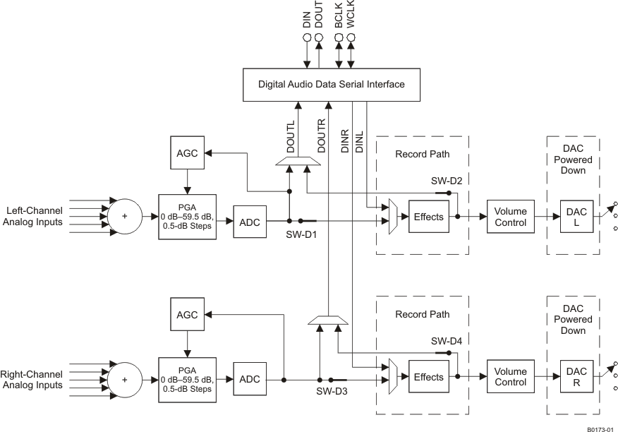
Digital Audio Processing for Record Path

In applications where record-only is selected, and DAC is powered down, the playback path signal processing blocks can be used in the ADC record path. These filtering blocks can support high-pass, low-pass, band-pass or notch filtering. In this mode, the record-only path has switches SW-D1 through SW-D4 closed, and reroutes the ADC output data through the digital signal processing blocks. Because the DAC digital signal processing blocks are being re-used, naturally the addresses of these digital filter coefficients are the same as for the DAC digital processing and are located on page 1, registers 1–52. This record-only mode is enabled by powering down both DACs by writing to page 0, register 37, bits D7–D6 (D7 = D6 = 0). Next, enable the digital filter pathway for the ADC by writing a 1 to page 0, register 107, bit D3. (Note, this pathway is only enabled if both DACs are powered down.) This record-only path is illustrated in Figure 10-22.
GUID-AEFA78A2-4A50-4700-BF39-A6F58846574E-low.gifFigure 10-22 Record-Only Mode With Digital Processing Path Enabled