SLOS630C December 2010 – November 2014 TLV320AIC3256
PRODUCTION DATA.
- 1 Features
- 2 Applications
- 3 Description
- 4 Simplified Block Diagram
- 5 Revision History
- 6 Device Comparison Table
- 7 Pin Configuration and Functions
-
8 Specifications
- 8.1 Absolute Maximum Ratings
- 8.2 Handling Ratings
- 8.3 Recommended Operating Conditions
- 8.4 Thermal Information
- 8.5 Electrical Characteristics, ADC
- 8.6 Electrical Characteristics, Bypass Outputs
- 8.7 Electrical Characteristics, Microphone Interface
- 8.8 Electrical Characteristics, Audio DAC Outputs
- 8.9 Electrical Characteristics, Misc.
- 8.10 Electrical Characteristics, Logic Levels
- 8.11 I2S/LJF/RJF Timing in Master Mode (see )
- 8.12 I2S/LJF/RJF Timing in Slave Mode (see )
- 8.13 DSP Timing in Master Mode (see )
- 8.14 DSP Timing in Slave Mode (see )
- 8.15 Digital Microphone PDM Timing (see )
- 8.16 I2C Interface Timing
- 8.17 SPI Interface Timing
- 8.18 Typical Characteristics
- 9 Parameter Measurement Information
- 10Detailed Description
- 11Application and Implementation
- 12Power Supply Recommendations
- 13Layout
- 14Device and Documentation Support
- 15Mechanical, Packaging, and Orderable Information
パッケージ・オプション
メカニカル・データ(パッケージ|ピン)
サーマルパッド・メカニカル・データ
- RSB|40
発注情報
13 Layout
13.1 Layout Guidelines
Each system design and PCB layout is unique. The layout should be carefully reviewed in the context of a specific PCB design. However, the following guidelines can optimize TLV320AIC3256 performance:
- Connect the thermal pad to ground.
- The decoupling capacitors for the power supplies should be placed close to the device terminals. Figure 21 shows the recommended decoupling capacitors for the TLV320AIC3256.
- Place the flying capacitor between FLY_P and FLY_N near the device terminals, with no VIAS in the trace between the device terminals and the capacitor. Similarly, keep the decoupling capacitor on VNEG near the device terminal with minimal VIAS in the trace between the device terminals, capacitor and PCB ground.
- The TLV320AIC3256 internal voltage references must be filtered using external capacitors. Place the filter capacitors on REF near the device terminals for optimal performance.
- The TLV320AIC3256 reduces crosstalk by a separate ground sense signal for the headphone jack. To optimize crosstalk performance, use a separate trace from the HPVSS_SENSE terminal to the headphone jack ground terminal, with no other ground connections along the length.
- For analog differential audio signals, the signals should be routed differentially on the PCB for better noise immunity. Avoid crossing of digital and analog signals to avoid undesirable crosstalk.
13.2 Layout Example
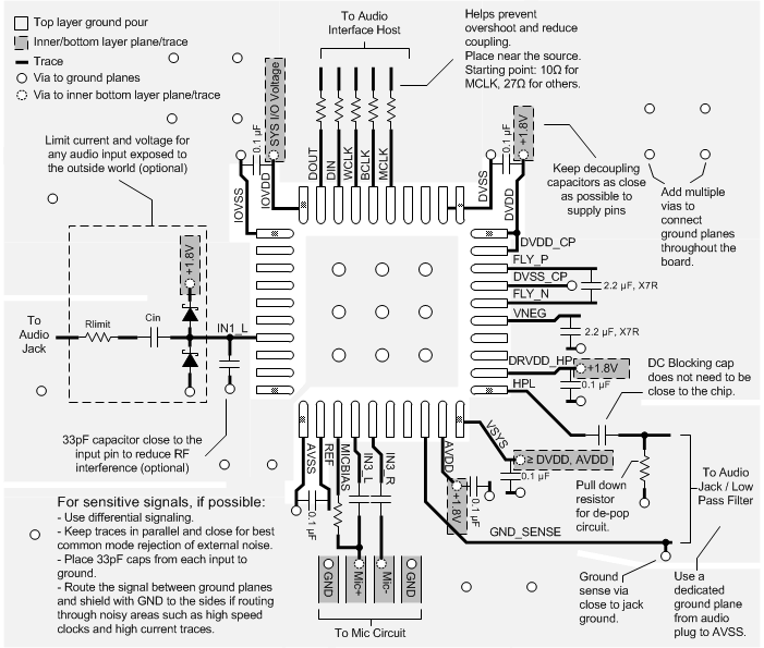 Figure 26. TLV320AIC3256 Layout
Example layout views can be found in the EVM User Guide: