SBOS751 December 2015 TLV2333 , TLV333 , TLV4333
PRODUCTION DATA.
- 1 Features
- 2 Applications
- 3 Description
- 4 Revision History
- 5 Device Comparison Table
- 6 Pin Configuration and Functions
- 7 Specifications
- 8 Detailed Description
- 9 Application and Implementation
- 10Power Supply Recommendations
- 11Layout
- 12Device and Documentation Support
- 13Mechanical, Packaging, and Orderable Information
パッケージ・オプション
メカニカル・データ(パッケージ|ピン)
サーマルパッド・メカニカル・データ
発注情報
8 Detailed Description
8.1 Overview
The TLVx333 series of low-cost operational amplifiers are unity-gain stable and free from unexpected output phase reversal. These devices use a proprietary auto-calibration technique to provide low offset voltage and very low drift over time and temperature. The TLVx333 family also offers rail-to-rail input and output and near-flat 1/f noise. These features make this series of op amps ideal for many applications and much easier to design into a wide variety of systems.
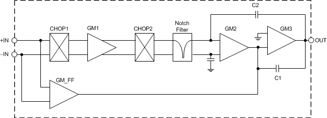
8.2 Functional Block Diagram

8.3 Feature Description
The TLV333, TLV2333, and TLV4333 are unity-gain stable, precision operational amplifiers free from unexpected output phase reversal. The use of proprietary zero-drift circuitry gives the benefit of low input offset voltage over time and temperature, as well as lowering the 1/f noise component. As a result of the high PSRR, these devices work well in applications that run directly from battery power without regulation. The TLV333 family is optimized for low-voltage, single-supply operation. These miniature, high-precision, low quiescent current amplifiers offer high-impedance inputs that have a common-mode range 100 mV beyond the supplies and a rail-to-rail output that swings within 100 mV of the supplies under normal test conditions. The TLV333 series are precision amplifiers for cost-sensitive applications.
8.3.1 Operating Voltage
The TLV333 series op amps can be used with single or dual supplies from an operating range of VS = 1.8 V (±0.9 V) up to 5.5 V (±2.75 V). Supply voltages greater than 7 V can permanently damage the device; see the Absolute Maximum Ratings table. Key parameters that vary over the supply voltage or temperature range are listed in the Typical Characteristics section.
8.3.2 Input Voltage
The TLV333, TLV2333, and TLV4333 input common-mode voltage range extends 0.1 V beyond the supply rails. The TLV333 is designed to cover the full range without the troublesome transition region found in some other rail-to-rail amplifiers.
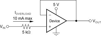
Typically, input bias current is approximately 200 pA; however, input voltages that exceed the power supplies can cause excessive current to flow into or out of the input pins. Momentary voltages greater than the power supply can be tolerated if the input current is limited to 10 mA. This limitation is easily accomplished with an input resistor, as shown in Figure 18.

NOTE:
A current-limiting resistor required if the input voltage exceeds the supply rails by ≥ 0.3 V.8.3.3 Internal Offset Correction
The TLV333, TLV2333, and TLV4333 op amps use an auto-calibration technique with a time-continuous, 125-kHz op amp in the signal path. This amplifier is zero-corrected every 8 µs using a proprietary technique. Upon power-up, the amplifier requires approximately 100 μs to achieve specified VOS accuracy. This design has no aliasing or flicker noise.
8.3.4 Achieving Output Swing to the Op Amp Negative Rail
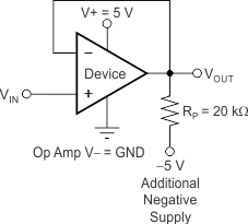
Some applications require output voltage swings from 0 V to a positive full-scale voltage (such as 2.5 V) with excellent accuracy. With most single-supply op amps, problems arise when the output signal approaches 0 V, near the lower output swing limit of a single-supply op amp. A good single-supply op amp can swing close to single-supply ground, but does not reach ground. The output of the TLV333, TLV2333, and TLV4333 can be made to swing to ground, or slightly below, on a single-supply power source. This swing to ground requires the use of another resistor and an additional, more negative, power supply than the op amp negative supply. Connect a pull-down resistor between the output and the additional negative supply to pull the output down below the value that the output can otherwise achieve, as shown in Figure 19.
 Figure 19. For VOUT Range to Ground
The TLV333, TLV2333, and TLV4333 have an output stage that allows the output voltage to be pulled to its negative supply rail, or slightly below, using the technique previously described. This technique only works with some types of output stages. The TLV333, TLV2333, and TLV4333 are characterized to perform with this technique; the recommended resistor value is approximately 20 kΩ. Note that this configuration increases the current consumption by several hundreds of microamps. Accuracy is excellent down to 0 V and as low as –2 mV. Limiting and nonlinearity occur below –2 mV, but excellent accuracy returns when the output is again driven above –2 mV. Lowering the resistance of the pull-down resistor allows the op amp to swing even further below the negative rail. Resistances as low as 10 kΩ can be used to achieve excellent accuracy down to –10 mV.
8.3.5 Input Differential Voltage
The typical input bias current of the TLV333 during normal operation is approximately 200 pA. In overdriven conditions, the bias current can increase significantly (see Figure 17).The most common cause of an overdriven condition occurs when the op amp is outside of the linear range of operation. When the output of the op amp is driven to one of the supply rails, the feedback loop requirements cannot be satisfied and a differential input voltage develops across the input pins. This differential input voltage results in activation of parasitic diodes inside the front-end input chopping switches that combine with 10-kΩ electromagnetic interference (EMI) filter resistors to create the equivalent circuit shown in Figure 20. Notice that the input bias current remains within specification within the linear region.
 Figure 20. Equivalent Input Circuit
8.3.6 EMI Susceptibility and Input Filtering
Operational amplifiers vary in their susceptibility to EMI. If conducted EMI enters the operational amplifier, the dc offset observed at the amplifier output may shift from its nominal value when EMI is present. This shift is a result of signal rectification associated with the internal semiconductor junctions. Although all operational amplifier pin functions can be affected by EMI, the input pins are likely to be the most susceptible. The TLV333 operational amplifier family incorporates an internal input low-pass filter that reduces the amplifier response to EMI. Both common-mode and differential mode filtering are provided by the input filter. The filter is designed for a cutoff frequency of approximately 8 MHz (–3 dB), with a roll-off of 20 dB per decade.
8.4 Device Functional Modes
The TLV333 devices have a single functional mode. These devices are powered on as long as the power-supply voltage is between 1.8 V (±0.9 V) and 5.5 V (±2.75 V).