JAJSNH8B December 2022 – September 2023 TLV2365 , TLV365
PRODUCTION DATA
- 1
- 1 特長
- 2 アプリケーション
- 3 概要
- 4 Revision History
- 5 Device Comparison Table
- 6 Pin Configuration and Functions
- 7 Specifications
- 8 Detailed Description
- 9 Application and Implementation
- 10Device and Documentation Support
- 11Mechanical, Packaging, and Orderable Information
6 Pin Configuration and Functions
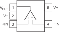
 Figure 6-1 TLV365 DBV Package,
5-Pin SOT-23 (Top View)
Figure 6-1 TLV365 DBV Package,
5-Pin SOT-23 (Top View)Table 6-1 Pin Functions: TLV365
| PIN | TYPE | DESCRIPTION | |
|---|---|---|---|
| NAME | NO. | ||
| –IN | 4 | Input | Negative (inverting) input |
| +IN | 3 | Input | Positive (noninverting) input |
| V– | 2 | — | Negative (lowest) power supply |
| V+ | 5 | — | Positive (highest) power supply |
| VOUT | 1 | Output | Output |
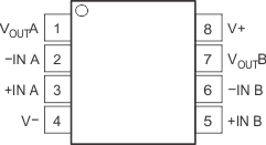
 Figure 6-2 TLV2365 D Package, 8-Pin SOIC (Top View)
Pin
Functions: TLV2365
| PIN | TYPE | DESCRIPTION | |
|---|---|---|---|
| NAME | NO. | ||
| –IN A | 2 | Input | Negative (inverting) input signal, channel A |
| +IN A | 3 | Input | Positive (noninverting) input signal, channel A |
| –IN B | 6 | Input | Negative (inverting) input signal, channel B |
| +IN B | 5 | Input | Positive (noninverting) input signal, channel B |
| V– | 4 | — | Negative (lowest) power supply |
| V+ | 8 | — | Positive (highest) power supply |
| VOUTA | 1 | Output | Output, channel A |
| VOUTB | 7 | Output | Output, channel B |