JAJSPA8 September 2020 TLV4011-Q1
PRODUCTION DATA
8.2.1.2 Detailed Design Procedure
Configure the circuit as shown in Figure 8-1. Note that VDD of the comparator is connected directly to VBAT (the battery being monitored) and the output of the comparator is level shifted with its open-drain ouput to 3.3 V which powers the micro-controller. Resistors R1 and R2 divide down VBAT so that the resistor divided output equals 1.226 V when VBAT reaches an undervoltage alert level of 2.0 V.
When the battery voltage sags down to 2.0 V, the resistor divider voltage crosses the (VIT = 1.226 V) threshold of the TLV4011-Q1. This causes the comparator output to transition from a logic high to a logic low. An open-drainj comparator is selected so the comparator output is compatible with the input logic level of the microcontroller. In addition, selecting a comparator with an integrated reference value of 1.226 V is favorable because it is the closest internal reference option that is less than the critical undervoltage level of 2.0 V. Choosing the internal reference option that is closest to the critical undervoltage level minimizes the resistor divider ratio which optimizes the accuracy of the circuit. Error at the falling edge threshold of (VIT) is amplified by the inverse of the resistor divider ratio. So minimizing the resistor divider ratio is a way of optimizing voltage monitoring accuracy.
Equation 1 is derived from the analysis of Figure 8-1.
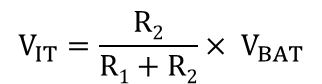
where
- R1 and R2 are the resistor values for the resistor divider connected to SENSE
- VBAT is the voltage source that is being monitored for an undervoltage condition.
- VIT is the falling edge threshold where the comparator output changes state from high to low
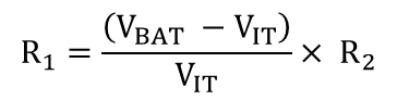
Rearranging Equation 1 and solving for R1 yields Equation 2.
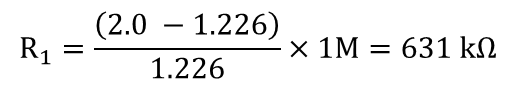
For the specific undervoltage detection of 2.0 V using the TLV4011-Q1, the following results are calculated.
where
- R2 is set to 1 MΩ
- VBAT is set to 2.0 V
- VIT is set to1.226 V
Choose RTOTAL (R1 + R2) such that the current through the divider is at approximately 100 times higher than the input bias current (IBIAS). The resistors can have high values to minimize current consumption in the circuit without adding significant error to the resistive divider.