JAJSPA9 October   2020 TLV4062-Q1 , TLV4082-Q1

PRODUCTION DATA  

  1. 特長
  2. アプリケーション
  3. 概要
  4. Revision History
  5. Pin Configuration and Functions
  6. Specifications
    1. 6.1 Absolute Maximum Ratings
    2. 6.2 ESD Ratings
    3. 6.3 Recommended Operating Conditions
    4. 6.4 Thermal Information
    5. 6.5 Electrical Characteristics
    6. 6.6 Timing Requirements
    7. 6.7 Timing Diagrams
    8. 6.8 Typical Characteristics
  7. Detailed Description
    1. 7.1 Overview
    2. 7.2 Functional Block Diagrams
    3. 7.3 Feature Description
    4. 7.4 Device Functional Modes
      1. 7.4.1 Inputs (IN1, IN2)
      2. 7.4.2 Outputs (OUT1, OUT2)
      3. 7.4.3 Switching Threshold and Hysteresis
  8. Application and Implementation
    1. 8.1 Application Information
      1. 8.1.1 Threshold Overdrive
    2. 8.2 Typical Applications
      1. 8.2.1 Monitoring Two Separate Rails
        1. 8.2.1.1 Design Requirements
        2. 8.2.1.2 Detailed Design Procedure
        3. 8.2.1.3 Application Curve
      2. 8.2.2 Early Warning Detection
        1. 8.2.2.1 Design Requirements
        2. 8.2.2.2 Detailed Design Procedure
        3. 8.2.2.3 Application Curve
      3. 8.2.3 Additional Application Information
        1. 8.2.3.1 Pull-Up Resistor Selection
        2. 8.2.3.2 INx Capacitor
  9. Power Supply Recommendations
  10. 10Layout
    1. 10.1 Layout Guidelines
    2. 10.2 Layout Example
  11. 11Device and Documentation Support
    1. 11.1 Documentation Support
      1. 11.1.1 Related Documentation
    2. 11.2 Receiving Notification of Documentation Updates
    3. 11.3 サポート・リソース
    4. 11.4 Trademarks
    5. 11.5 静電気放電に関する注意事項
    6. 11.6 用語集
      1.      Mechanical, Packaging, and Orderable Information

パッケージ・オプション

メカニカル・データ(パッケージ|ピン)
サーマルパッド・メカニカル・データ
発注情報

Functional Block Diagrams

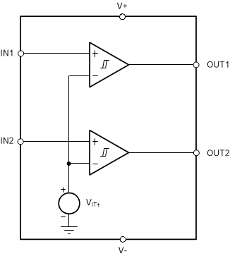
GUID-6532C254-5487-4630-BBDF-480E876E2FAB-low.gifFigure 7-1 TLV4062-Q1 (Push-Pull Output) Block Diagram
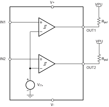
GUID-0BB36B28-8611-4CDA-8360-71DF2ECCB501-low.gifFigure 7-2 TLV4082-Q1 (Open-Drain Output) Block Diagram