SBOS935B April 2020 – July 2020 TLV197-Q1 , TLV2197-Q1 , TLV4197-Q1
PRODUCTION DATA.
- 1 Features
- 2 Applications
- 3 Description
- 4 Revision History
- 5 Pin Configuration and Functions
-
6 Specifications
- 6.1 Absolute Maximum Ratings
- 6.2 ESD Ratings
- 6.3 Recommended Operating Conditions
- 6.4 Thermal Information: TLV197-Q1
- 6.5 Thermal Information: TLV2197-Q1
- 6.6 Thermal Information: TLV4197-Q1
- 6.7 Electrical Characteristics: VS = ±4 V to ±18 V (VS = 8 V to 36 V)
- 6.8 Electrical Characteristics: VS = ±2.25 V to ±4 V (VS = 4.5 V to 8 V)
- 6.9 Typical Characteristics
- 7 Detailed Description
- 8 Application and Implementation
- 9 Power Supply Recommendations
- 10Layout
- 11Device and Documentation Support
- 12Mechanical, Packaging, and Orderable Information
7.3.5 Capacitive Load and Stability
The TLVx197-Q1 features a patented output stage capable of driving large capacitive loads, and in a unity-gain configuration, directly drives up to 1 nF of pure capacitive load. Increasing the gain enhances the ability of the amplifier to drive greater capacitive loads.
The particular op amp circuit configuration, layout, gain, and output loading are some of the factors to consider when establishing whether an amplifier is stable in operation.
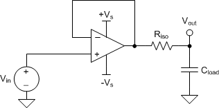
For additional drive capability in unity-gain configurations, improve capacitive load drive by inserting a small (10-Ω to 20-Ω) resistor, RISO, in series with the output, as shown in Figure 38. This resistor significantly reduces ringing and maintains dc performance for purely capacitive loads. However, if a resistive load is in parallel with the capacitive load, then a voltage divider is created, thus introducing a gain error at the output and slightly reducing the output swing. The error introduced is proportional to the ratio RISO / RL, and is generally negligible at low output levels. A high capacitive load drive makes the TLVx197-Q1 a great choice for applications such as reference buffers, MOSFET gate drives, and cable-shield drives. The circuit shown in Figure 38 uses an isolation resistor, RISO, to stabilize the output of an op amp. RISO modifies the open-loop gain of the system for increased phase margin, and the results using the TLVx197-Q1 are summarized in Table 2. For additional information on techniques to optimize and design using this circuit, reference design TIPD128, Capacitive Load Drive Verified Reference Design Using an Isolation Resistor, details complete design goals, simulation, and test results.
 Figure 38. Extending Capacitive Load Drive With the TLVx197-Q1
 Table 2. TLVx197-Q1 Capacitive Load Drive Using Isolation Resistor Comparison of Calculated and Measured Results
| PARAMETER | VALUE | |||||||||
|---|---|---|---|---|---|---|---|---|---|---|
| Capacitive Load | 100 pF | 1000 pF | 0.01 µF | 0.1 µF | 1 µF | |||||
| Phase Margin | 45° | 60° | 45° | 60° | 45° | 60° | 45° | 60° | 45° | 60° |
| RISO (Ω) | 47 | 360 | 24 | 100 | 20 | 51 | 6.2 | 15.8 | 2 | 4.7 |
| Measured Overshoot (%) | 23.2 8.6 | 10.4 | 22.5 | 9 | 22.1 | 8.7 | 23.1 | 8.6 | 21 | 8.6 |
| Calculated PM | 45.1° | 58.1° | 45.8° | 59.7° | 46.1° | 60.1° | 45.2° | 60.2° | 47.2° | 60.2° |
| For step-by-step design procedure, circuit schematics, bill of materials, printed circuit board (PCB) files, simulation results, and test results, see TI Precision Design TIDU032, Capacitive Load Drive Solution using an Isolation Resistor . |