SLVSBC1D October   2013  – October 2016 TLV62565 , TLV62566

PRODUCTION DATA.  

  1. Features
  2. Applications
  3. Description
  4. Simplified Schematic
  5. Revision History
  6. Device Comparison Table
  7. Pin Configuration and Functions
  8. Specifications
    1. 8.1 Absolute Maximum Ratings
    2. 8.2 ESD Ratings
    3. 8.3 Recommended Operating Conditions
    4. 8.4 Thermal Information
    5. 8.5 Electrical Characteristics
    6. 8.6 Typical Characteristics
  9. Detailed Description
    1. 9.1 Overview
    2. 9.2 Functional Block Diagrams
    3. 9.3 Feature Description
      1. 9.3.1 Power Save Mode
      2. 9.3.2 Enabling/Disabling the Device
      3. 9.3.3 Soft Start
      4. 9.3.4 Switch Current Limit
      5. 9.3.5 Power Good
    4. 9.4 Device Functional Modes
      1. 9.4.1 Under Voltage Lockout
      2. 9.4.2 Thermal Shutdown
  10. 10Application and Implementation
    1. 10.1 Application Information
    2. 10.2 Typical Application
      1. 10.2.1 Design Requirements
        1. 10.2.1.1 Output Filter Design
        2. 10.2.1.2 Inductor Selection
        3. 10.2.1.3 Input and Output Capacitor Selection
      2. 10.2.2 Detailed Design Procedure
        1. 10.2.2.1 Setting the Output Voltage
        2. 10.2.2.2 Loop Stability
      3. 10.2.3 Application Performance Curves
  11. 11Power Supply Recommendations
  12. 12Layout
    1. 12.1 Layout Guidelines
    2. 12.2 Layout Example
    3. 12.3 Thermal Considerations
  13. 13Device and Documentation Support
    1. 13.1 Device Support
      1. 13.1.1 Third-Party Products Disclaimer
    2. 13.2 Documentation Support
      1. 13.2.1 Related Documentation
    3. 13.3 Related Links
    4. 13.4 Receiving Notification of Documentation Updates
    5. 13.5 Community Resources
    6. 13.6 Trademarks
    7. 13.7 Electrostatic Discharge Caution
    8. 13.8 Glossary
  14. 14Mechanical, Packaging, and Orderable Information

パッケージ・オプション

メカニカル・データ(パッケージ|ピン)
サーマルパッド・メカニカル・データ
発注情報

7 Pin Configuration and Functions

5-Pin SOT-23
DBV Package
(Top View)
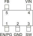
TLV62565 TLV62566 TLV62565_pin_assign.gif

Pin Functions

PIN I/O/PWR DESCRIPTION
NAME NUMBER
TLV62565 TLV62566
EN 1 I Device enable logic input. Logic HIGH enables the device, logic low disables the device and turns it into shutdown. Do not leave floating.
FB 5 5 I Feedback pin for the internal control loop. Connect this pin to the external feedback divider.
GND 2 2 PWR Ground pin.
PG 1 O Power Good open drain output. This pin is high impedance if the output voltage is within regulation. It is pulled low if the output is below its nominal value. It is also low when VIN is below UVLO or thermal shutdown triggers.
SW 3 3 PWR Switch pin connected to the internal MOSFET switches and inductor terminal. Connect the inductor of the output filter to this pin.
VIN 4 4 PWR Power supply voltage input.