JAJSEJ9B January   2018  – October 2018 TLV6710

PRODUCTION DATA.  

  1. 特長
  2. アプリケーション
  3. 概要
    1.     Device Images
      1.      ブロック概略図
  4. 改訂履歴
  5. デバイス比較表
  6. Pin Configuration and Functions
    1.     Pin Functions
  7. Specifications
    1. 7.1 Absolute Maximum Ratings
    2. 7.2 ESD Ratings
    3. 7.3 Recommended Operating Conditions
    4. 7.4 Thermal Information
    5. 7.5 Electrical Characteristics
    6. 7.6 Timing Requirements
    7. 7.7 Typical Characteristics
  8. Detailed Description
    1. 8.1 Overview
    2. 8.2 Functional Block Diagram
    3. 8.3 Feature Description
      1. 8.3.1 Inputs (INA, INB)
      2. 8.3.2 Outputs (OUTA, OUTB)
    4. 8.4 Device Functional Modes
      1. 8.4.1 Normal Operation (VDD > UVLO)
      2. 8.4.2 Undervoltage Lockout (V(POR) < VDD < UVLO)
      3. 8.4.3 Power On Reset (VDD < V(POR))
  9. Application and Implementation
    1. 9.1 Application Information
      1. 9.1.1 Window Comparator Considerations
      2. 9.1.2 Input and Output Configurations
      3. 9.1.3 Immunity to Input Pin Voltage Transients
    2. 9.2 Typical Application
      1. 9.2.1 Design Requirements
      2. 9.2.2 Detailed Design Procedure
      3. 9.2.3 Application Curve
    3. 9.3 Do's and Don'ts
  10. 10Power Supply Recommendations
  11. 11Layout
    1. 11.1 Layout Guidelines
    2. 11.2 Layout Example
  12. 12デバイスおよびドキュメントのサポート
    1. 12.1 デバイス・サポート
      1. 12.1.1 開発サポート
    2. 12.2 ドキュメントのサポート
      1. 12.2.1 関連資料
    3. 12.3 ドキュメントの更新通知を受け取る方法
    4. 12.4 コミュニティ・リソース
    5. 12.5 商標
    6. 12.6 静電気放電に関する注意事項
    7. 12.7 Glossary
  13. 13メカニカル、パッケージ、および注文情報

パッケージ・オプション

メカニカル・データ(パッケージ|ピン)
サーマルパッド・メカニカル・データ
発注情報

Typical Characteristics

At TJ = 25°C and VDD = 12 V, unless otherwise noted.
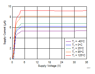
TLV6710 D001_snvsav4.gif
Figure 2. Supply Current vs Supply Voltage
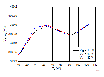
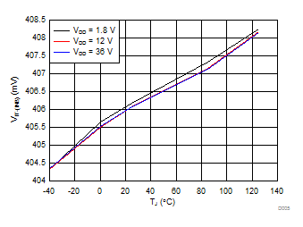
TLV6710 D005_snvsav4.gifFigure 4. INA Positive Input Threshold Voltage (VIT+(INA)) vs Temperature
TLV6710 D004_snvsav4.gif
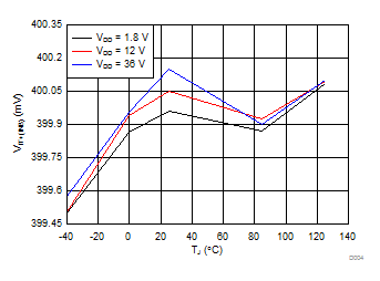
Figure 6. INB Positive Input Threshold Voltage (VIT+(INB)) vs Temperature
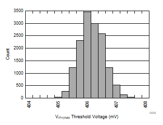
TLV6710 D022_snvsav4.gif
VDD = 1.8 V
Figure 8. INA Positive Input Threshold Voltage (VIT+(INA)) Distribution
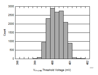
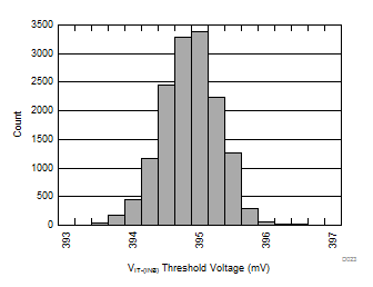
TLV6710 D021_snvsav4.gif
VDD = 1.8 V
Figure 10. INB Positive Input Threshold Voltage (VIT+(INB)) Distribution
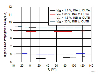
TLV6710 D007_snvsav4.gif
Input step ±200 mV
Figure 12. Propagation Delay vs Temperature
(High-to-Low Transition at the Inputs)
TLV6710 D009_snvsav4.gif
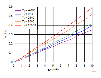
VDD = 1.8 V
Figure 14. Output Voltage Low vs Output Sink Current
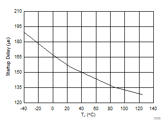
TLV6710 D025_snvsav4.gif
VDD = 5 V
Figure 16. Start-Up Delay vs Temperature
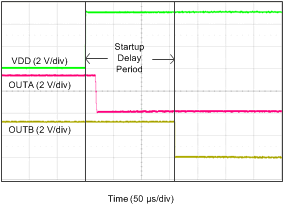
TLV6710 StartupDelay4.gif
VDD = 5 V, VINA = 410 mV, VINB = 390 mV, VPULLUP = 3.3 V
Figure 18. Start-Up Delay
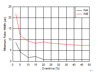
TLV6710 D011_snvsav4.gif
VDD = 24 V
Figure 3. Minimum Pulse Duration vs
Threshold Overdrive Voltage(1)(1)
TLV6710 D002_snvsav4.gifFigure 5. INA Negative Input Threshold Voltage (VIT–(INA)) vs Temperature
TLV6710 D003_snvsav4.gif
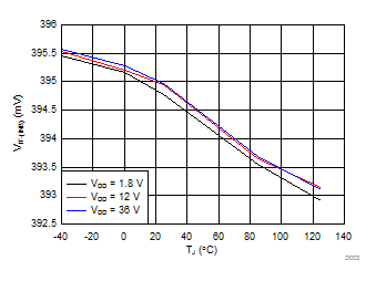
Figure 7. INB Negative Input Threshold Voltage (VIT–(INB)) vs Temperature
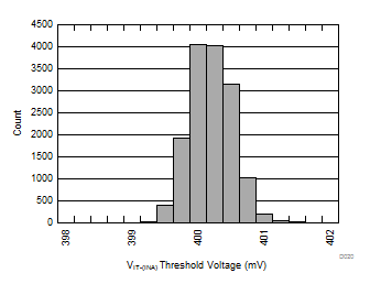
TLV6710 D020_snvsav4.gif
VDD = 1.8 V
Figure 9. INA Negative Input Threshold Voltage (VIT–(INA)) Distribution
TLV6710 D023_snvsav4.gif
VDD = 1.8 V
Figure 11. INB Negative Input Threshold Voltage (VIT–(INB)) Distribution
TLV6710 D008_snvsav4.gif
Input step ±200 mV
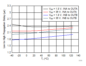
Figure 13. Propagation Delay vs Temperature
(Low-to-High Transition at the Inputs)
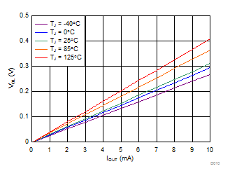
TLV6710 D010_snvsav4.gif
VDD = 12 V
Figure 15. Output Voltage Low vs Output Sink Current
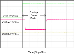
TLV6710 StartupDelay5.gif
VDD = 5 V, VINA = 390 mV, VINB = 410 mV, VPULLUP = 3.3 V
Figure 17. Start-Up Delay
Minimum pulse duration required to trigger output high-to-low transition. INA = negative spike below VIT– and INB = positive spike above VIT+.