JAJSFH0G february   2011  – june 2023 TLV707 , TLV707P

PRODUCTION DATA  

  1.   1
  2. 特長
  3. アプリケーション
  4. 概要
  5. Revision History
  6. Pin Configuration and Functions
  7. Specifications
    1. 6.1 Absolute Maximum Ratings
    2. 6.2 ESD Ratings
    3. 6.3 Recommended Operating Conditions
    4. 6.4 Thermal Information
    5. 6.5 Electrical Characteristics
    6. 6.6 Typical Characteristics
  8. Detailed Description
    1. 7.1 Overview
    2. 7.2 Functional Block Diagrams
    3. 7.3 Feature Description
      1. 7.3.1 Internal Current Limit
      2. 7.3.2 Shutdown
    4. 7.4 Device Functional Modes
  9. Application and Implementation
    1. 8.1 Application Information
    2. 8.2 Typical Application
      1. 8.2.1 Design Requirements
      2. 8.2.2 Detailed Design Procedure
        1. 8.2.2.1 Input and Output Capacitor Requirements
        2. 8.2.2.2 Dropout Voltage
        3. 8.2.2.3 Transient Response
      3. 8.2.3 Application Curves
    3. 8.3 Best Design Practices
    4. 8.4 Power Supply Recommendations
    5. 8.5 Layout
      1. 8.5.1 Layout Guidelines
        1. 8.5.1.1 Board Layout Recommendations to Improve PSRR and Noise Performance
        2. 8.5.1.2 Package Mounting
        3. 8.5.1.3 Thermal Considerations
        4. 8.5.1.4 Power Dissipation
      2. 8.5.2 Layout Example
  10. Device and Documentation Support
    1. 9.1 Device Support
      1. 9.1.1 Development Support
        1. 9.1.1.1 Evaluation Modules
        2. 9.1.1.2 Spice Models
      2. 9.1.2 Device Nomenclature
    2. 9.2 Documentation Support
      1. 9.2.1 Related Documentation
    3. 9.3 ドキュメントの更新通知を受け取る方法
    4. 9.4 サポート・リソース
    5. 9.5 Trademarks
    6. 9.6 静電気放電に関する注意事項
    7. 9.7 用語集
  11. 10Mechanical, Packaging, and Orderable Information

パッケージ・オプション

メカニカル・データ(パッケージ|ピン)
サーマルパッド・メカニカル・データ
発注情報

Typical Characteristics

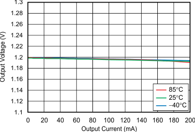
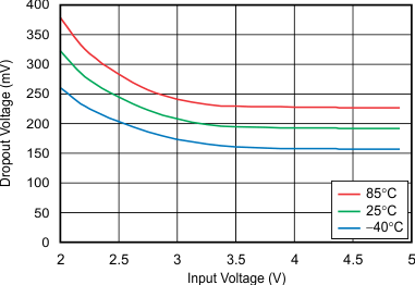
at TJ = –40°C to +85°C, VIN = VOUT(nom) + 0.5 V or 2.0 V (whichever is greater), IOUT = 10 mA, VEN = VIN, and COUT = 1 μF (unless otherwise noted); typical values are at TJ = 25°C
GUID-A3DB9861-D902-432C-9701-05A9361CEA28-low.gif
VOUT = 1.2 V
Figure 6-1 Load Regulation
GUID-6FD4B64F-F4F7-4365-B187-83F52542F7D6-low.gif
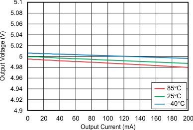
VOUT = 5.0 V
Figure 6-3 Load Regulation
GUID-DCDFD670-B419-4C7E-8A77-1442F690AEF5-low.gif
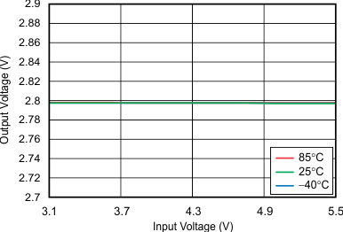
VOUT = 2.8 V, IOUT = 10 mA
Figure 6-5 Line Regulation
GUID-A995CD44-60C1-4E36-B3F7-174E29E9DA19-low.gif
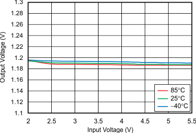
VOUT = 1.2 V, IOUT = 150 mA
Figure 6-7 Line Regulation
GUID-CEA6397A-FA65-4D70-9CA5-32817C1E03D2-low.gif
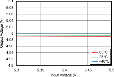
VOUT = 5.0 V, IOUT = 150 mA
Figure 6-9 Line Regulation
GUID-D8DF531A-B7BF-4676-AEDA-363B4DA23097-low.gif
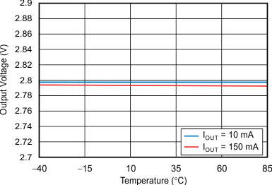
VOUT = 2.8 V
Figure 6-11 Output Voltage vs Temperature
GUID-F6E11243-E04C-457C-BD1A-0CAE9924E594-low.gif
IOUT = 150 mA
Figure 6-13 Dropout Voltage vs Input Voltage
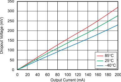
GUID-3271069D-CC35-4B36-95A5-ECB389F21E63-low.gif
VOUT = 2.8 V
Figure 6-15 Dropout Voltage vs Output Current
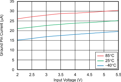
GUID-333B59B6-317C-4825-BF60-9B7813F25726-low.gif
VOUT = 1.2 V, IOUT = 0 mA
Figure 6-17 Ground Pin Current vs Input Voltage
GUID-9963A6B7-0575-42D6-87F0-09E24B5C19FB-low.gif
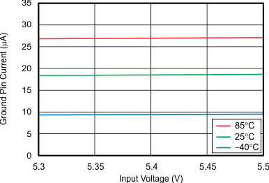
VOUT = 5.0 V, IOUT = 0 mA
Figure 6-19 Ground Pin Current vs Input Voltage
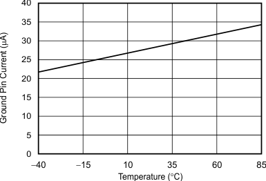
GUID-342770CE-EEB8-4726-A3A0-EBF3D6303FB2-low.gif
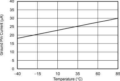
VOUT = 2.8 V, IOUT = 0 mA
Figure 6-21 Ground Pin Current vs Temperature
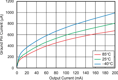
GUID-5CB252B1-5E6D-4C95-978C-6344B66DB60E-low.gif
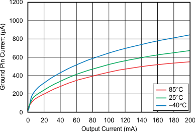
VOUT = 1.2 V
Figure 6-23 Ground Pin Current vs Output Current
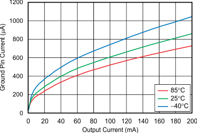
GUID-B6D2686A-CB7C-4D87-A0DD-4C0879132921-low.gif
VOUT = 5.0 V
Figure 6-25 Ground Pin Current vs Output Current
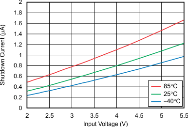
GUID-16CF916D-C48D-41C1-BDE1-2F5FC9C3EA80-low.gif
VOUT = 2.8 V
Figure 6-27 Shutdown Current vs Input Voltage
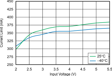
GUID-84F89337-331F-465D-8F7E-6E21C84C836C-low.gif
VOUT = 1.2 V
Figure 6-29 Current Limit vs Input Voltage
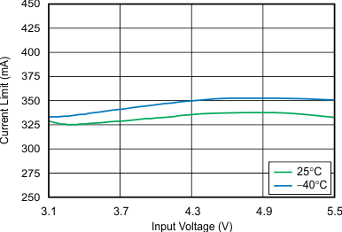
GUID-DDF6506D-761F-49CD-AE6B-B741766FC162-low.gif
VOUT = 5.0 V
Figure 6-31 Current Limit vs Input Voltage
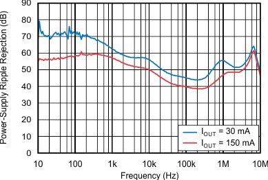
GUID-FF580703-D7C4-4E8D-8BAB-17C411FA0C7C-low.gif
VOUT = 2.8 V
Figure 6-33 Power-Supply Ripple Rejection vs Frequency
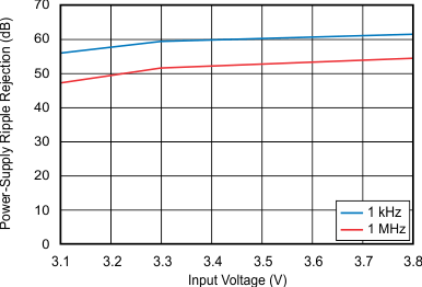
GUID-BA430005-AD21-47E6-B5BE-DEAFE2424381-low.gif
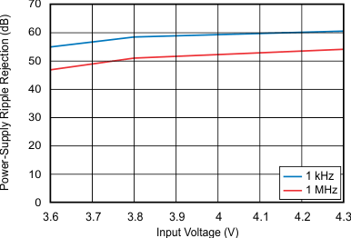
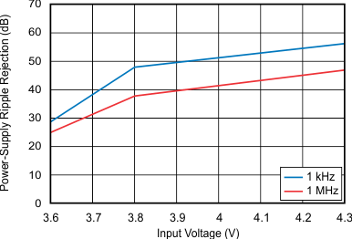
VOUT = 2.8 V, IOUT = 30 mA
Figure 6-35 Power-Supply Ripple Rejection vs Input Voltage
GUID-0DC1D3F1-743F-4B64-B1CB-F0BA2EBE972B-low.gif
VOUT = 3.3 V, IOUT = 30 mA
Figure 6-37 Power-Supply Ripple Rejection vs Input Voltage
GUID-3018FDFB-E5A6-4A4C-ACC2-1669314C26E0-low.gif
 
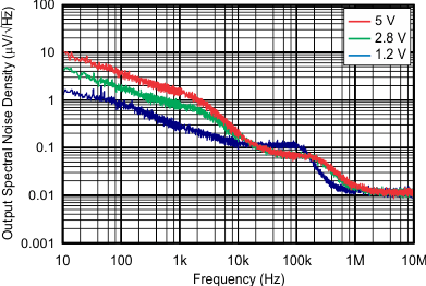
Figure 6-39 Output Spectral Noise Density vs Frequency
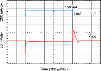
GUID-BCF0A2A5-FC89-4ACB-B829-18E059E4DBC1-low.gif
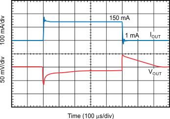
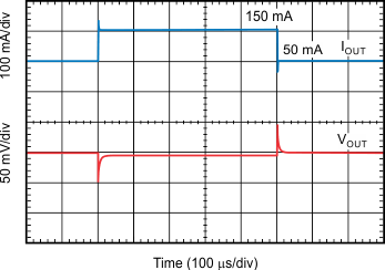
VOUT = 1.2 V
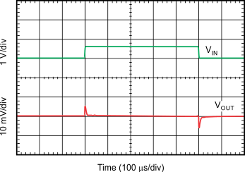
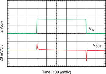
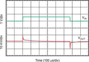
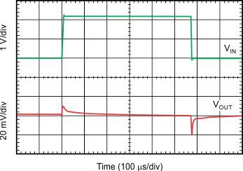
Figure 6-41 Load Transient Response
GUID-9D401DB6-0EA9-4E08-8C38-BB442426CE6D-low.gif
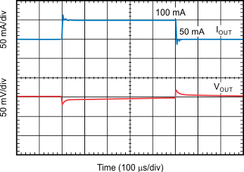
VOUT = 2.8 V
Figure 6-43 Load Transient Response
GUID-E8E57CE9-F15B-4DF3-BAA2-E3393562232D-low.gif
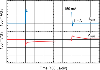
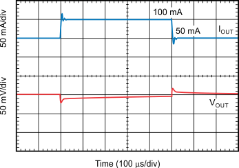
VOUT = 5.0 V
Figure 6-45 Load Transient Response
GUID-46CFA46D-C456-4A69-9237-178B1C81300F-low.gif
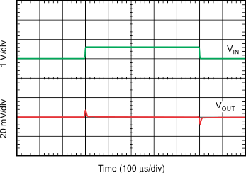
VOUT = 1.2 V, IOUT = 200 mA
Figure 6-47 Line Transient Response
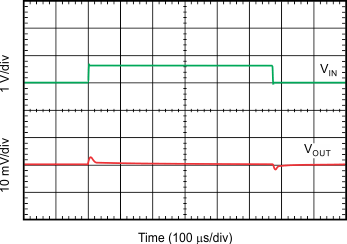
GUID-BC285BB6-C9FE-4376-93BD-6AA6B9AA3BB6-low.gif
VOUT = 1.2 V, IOUT = 200 mA
Figure 6-49 Line Transient Response
GUID-F6B91277-A353-48BA-A8A1-781A8EADA6B1-low.gif
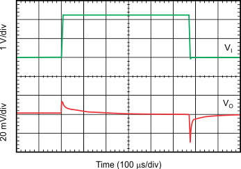
VOUT = 2.8 V, IOUT = 200 mA
Figure 6-51 Line Transient Response
GUID-1547C300-B170-4DC6-8C76-43A2E08A6E63-low.gif
VOUT = 2.8 V, IOUT = 200 mA
Figure 6-53 Line Transient Response
GUID-D843580E-D69C-4631-892B-D7E9E4266A73-low.gif
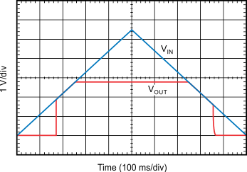
VOUT = 2.8 V, IOUT = 30 mA
Figure 6-55 VIN Ramp Up, Ramp Down Response
GUID-83F29CD2-9CD2-4F6C-A5B6-61C26E248895-low.gif
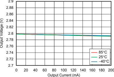
VOUT = 2.8 V
Figure 6-2 Load Regulation
GUID-AA60C129-554A-454B-9001-C50B1E33D8D3-low.gif
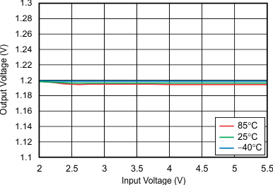
VOUT = 1.2 V, IOUT = 10 mA
Figure 6-4 Line Regulation
GUID-0D2C8F89-B3C1-4647-BFE5-BEABFDCBADFE-low.gif
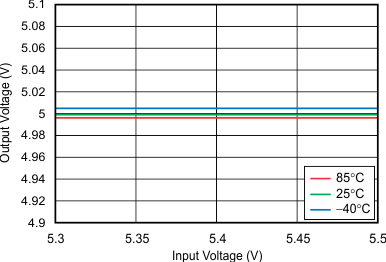
VOUT = 5.0 V, IOUT = 10 mA
Figure 6-6 Line Regulation
GUID-D7EA0C2C-6530-432B-834A-855473A2FBF7-low.gif
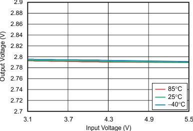
VOUT = 2.8 V, IOUT = 150 mA
Figure 6-8 Line Regulation
GUID-D2455C3E-0EAE-4B9E-8324-966ABA70F59C-low.gif
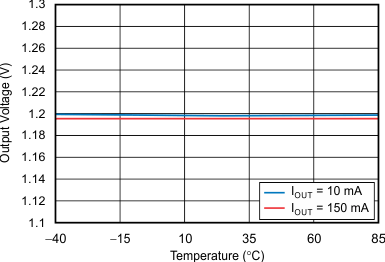
VOUT = 1.2 V
Figure 6-10 Output Voltage vs Temperature
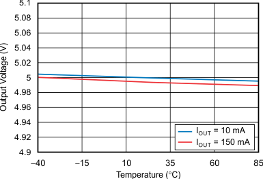
GUID-DF21E002-5F68-4469-8879-2E14E3EDEF69-low.gif
VOUT = 5.0 V
Figure 6-12 Output Voltage vs Temperature
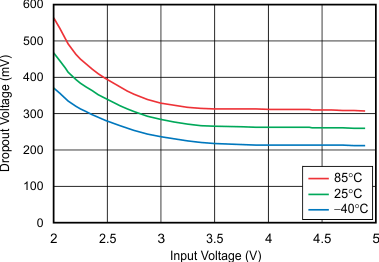
GUID-E43F6147-7260-42F0-9D9F-CE2BA58D8764-low.gif
IOUT = 200 mA
Figure 6-14 Dropout Voltage vs Input Voltage
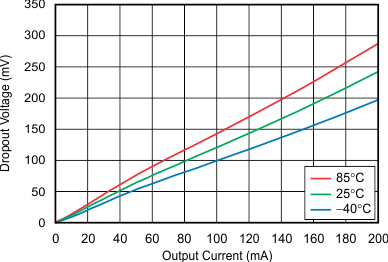
GUID-1E466116-E89D-4103-A3AD-30973921D045-low.gif
VOUT = 5.0 V
Figure 6-16 Dropout Voltage vs Output Current
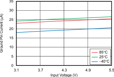
GUID-44F98F08-94AF-4887-ACAF-5BE3F1D8E63D-low.gif
VOUT = 2.8 V, IOUT = 0 mA
Figure 6-18 Ground Pin Current vs Input Voltage
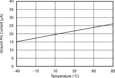
GUID-144A95E0-4E79-4C6E-A29D-E48A7EF58044-low.gif
VOUT = 1.2 V, IOUT = 0 mA
Figure 6-20 Ground Pin Current vs Temperature
GUID-D3430368-6BCF-4A9C-B596-9408DCD34ADA-low.gif
VOUT = 5.0 V, IOUT = 0 mA
Figure 6-22 Ground Pin Current vs Temperature
GUID-5D78A24B-CABD-4C21-A458-670F0E88FA2A-low.gif
VOUT = 2.8 V
Figure 6-24 Ground Pin Current vs Output Current
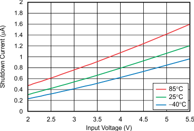
GUID-311C44AE-2626-47B1-B459-C82B03684BC1-low.gif
VOUT = 1.2 V
Figure 6-26 Shutdown Current vs Input Voltage
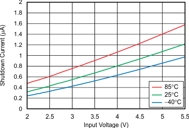
GUID-B9365E10-B1E1-4943-A14C-560CBD2DE960-low.gif
VOUT = 5.0 V
Figure 6-28 Shutdown Current vs Input Voltage
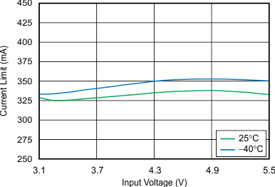
GUID-E9A127EF-8434-45BC-B323-160500C0A2DE-low.gif
VOUT = 2.8 V
Figure 6-30 Current Limit vs Input Voltage
GUID-7C1FFEE7-FF89-4534-BBFE-4C17FD3B3A92-low.gif
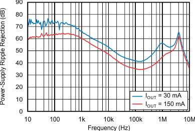
VOUT = 1.2 V
Figure 6-32 Power-Supply Ripple Rejection vs Frequency
GUID-CE14F075-BC59-459A-B783-88E9E18655D3-low.gif
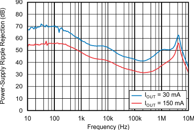
VOUT = 5.0 V
Figure 6-34 Power-Supply Ripple Rejection vs Frequency
GUID-CD609C55-CFA1-49F3-AEAA-0EAB729C1E24-low.gif
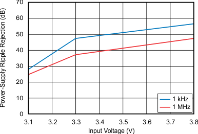
VOUT = 2.8 V, IOUT = 150 mA
Figure 6-36 Power-Supply Ripple Rejection vs Input Voltage
GUID-375FDDD3-DE80-4450-B4D4-65132C79CC44-low.gif
VOUT = 3.3 V, IOUT = 150 mA
Figure 6-38 Power-Supply Ripple Rejection vs Input Voltage
GUID-E55DADB7-EA63-411A-9C56-051AFF81AD5B-low.gif
VOUT = 1.2 V
Figure 6-40 Load Transient Response
GUID-4B2952E5-9DAE-4B54-ABFD-4C4B1281CC27-low.gif
VOUT = 2.8 V
Figure 6-42 Load Transient Response
GUID-4F39836A-D688-4C2A-8CAE-AE5957F84B50-low.gif
VOUT = 5.0 V
Figure 6-44 Load Transient Response
GUID-D0C7D043-0F3E-444F-8253-36F650FE0EA8-low.gif
VOUT = 1.2 V, IOUT = 150 mA
Figure 6-46 Line Transient Response
GUID-792CA5F4-675D-4D6B-AAEA-9D289B24F92D-low.gif
VOUT = 1.2 V, IOUT = 150 mA
Figure 6-48 Line Transient Response
GUID-265ED08B-1AD7-4D1B-A2B3-F48A369E3B2F-low.gif
VOUT = 2.8 V, IOUT = 150 mA
Figure 6-50 Line Transient Response
GUID-7D47F400-6DF3-4FEF-81DB-6C44894978B8-low.gif
VOUT = 2.8 V, IOUT = 200 mA
Figure 6-52 Line Transient Response
GUID-FF2B1663-55C8-4635-BBD7-872D6174E39A-low.gif
VOUT = 1.2 V, IOUT = 30 mA
Figure 6-54 VIN Ramp Up, Ramp Down Response
GUID-B6F80E92-5A31-4B9D-B5E6-A3649A3365BA-low.gif
VOUT = 5 V, IOUT = 30 mA
Figure 6-56 VIN Ramp Up, Ramp Down Response