JAJSCK4A October   2016  – November 2016 TLV8811 , TLV8812

PRODUCTION DATA.  

  1. 特長
  2. アプリケーション
  3. 概要
  4. 改訂履歴
  5. Pin Configuration and Functions
  6. Specifications
    1. 6.1 Absolute Maximum Ratings
    2. 6.2 ESD Ratings
    3. 6.3 Recommended Operating Conditions
    4. 6.4 Thermal Information
    5. 6.5 Electrical Characteristics
    6. 6.6 Typical Characteristics
  7. Detailed Description
    1. 7.1 Overview
    2. 7.2 Functional Block Diagram
    3. 7.3 Feature Description
    4. 7.4 Device Functional Modes
      1. 7.4.1 Negative-Rail Sensing Input
      2. 7.4.2 Rail to Rail Output Stage
      3. 7.4.3 Design Optimization for Nanopower Operation
      4. 7.4.4 Driving Capacitive Load
  8. Application and Implementation
    1. 8.1 Application Information
    2. 8.2 Typical Application: Three Terminal CO Gas Sensor Amplifier
      1. 8.2.1 Design Requirements
      2. 8.2.2 Detailed Design Procedure
      3. 8.2.3 Application Curve
    3. 8.3 Do's and Don'ts
  9. Power Supply Recommendations
  10. 10Layout
    1. 10.1 Layout Guidelines
    2. 10.2 Layout Example
  11. 11デバイスおよびドキュメントのサポート
    1. 11.1 デバイス・サポート
      1. 11.1.1 開発サポート
    2. 11.2 ドキュメントのサポート
      1. 11.2.1 関連資料
    3. 11.3 関連リンク
    4. 11.4 ドキュメントの更新通知を受け取る方法
    5. 11.5 コミュニティ・リソース
    6. 11.6 商標
    7. 11.7 静電気放電に関する注意事項
    8. 11.8 用語集
  12. 12メカニカル、パッケージ、および注文情報

パッケージ・オプション

メカニカル・データ(パッケージ|ピン)
サーマルパッド・メカニカル・データ
発注情報

Pin Configuration and Functions

TLV8811 5-Pin SOT-23
DBV Package
Top View
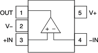
TLV8811 TLV8812 po_333_sot23_bos351.gif
TLV8812 8-Pin VSSOP
DGK Package
Top View
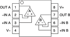
TLV8811 TLV8812 po_2333_so_msop_bos351.gif

Pin Functions: TLV8811 DBV

PIN TYPE DESCRIPTION
NAME NUMBER
OUT 1 O Output
-IN 4 I Inverting Input
+IN 3 I Non-Inverting Input
V- 2 P Negative (lowest) power supply
V+ 5 P Positive (highest) power supply

Pin Functions: TLV8812 DGK

PIN TYPE DESCRIPTION
NAME NUMBER
OUT A 1 O Channel A Output
-IN A 2 I Channel A Inverting Input
+IN A 3 I Channel A Non-Inverting Input
V- 4 P Negative (lowest) power supply
+IN B 5 I Channel B Non-Inverting Input
-IN B 6 I Channel B Inverting Input
OUT B 7 O Channel B Output
V+ 8 P Positive (highest) power supply