JAJSJ20A June   2020  – October 2020 TMAG5124

PRODUCTION DATA  

  1.   1
  2. 特長
  3. アプリケーション
  4. 概要
  5. Revision History
  6. Device Comparison Table
  7. Pin Configuration and Functions
  8. Specifications
    1. 7.1 Absolute Maximum Ratings
    2. 7.2 ESD Ratings
    3. 7.3 Recommended Operating Conditions
    4. 7.4 Thermal Information
    5. 7.5 Electrical Characteristics
    6. 7.6 Magnetic Characteristics
    7. 7.7 Typical Characteristics
      1. 7.7.1 TMAG5124A and TMAG5124E
      2. 7.7.2 TMAG5124B and TMAG5124F
      3. 7.7.3 TMAG5124C and TMAG5124G
      4. 7.7.4 TMAG5124D and TMAG5124H
      5. 7.7.5 Current Output Level
        1. 7.7.5.1 Low-Level Current Output for TMAG5124A/B/C/D
        2. 7.7.5.2 Low-Level Current Output for TMAG5124E/F/G/H
        3. 7.7.5.3 High-Level Current Output for Every Version
  9. Detailed Description
    1. 8.1 Overview
    2. 8.2 Functional Block Diagram
    3. 8.3 Feature Description
      1. 8.3.1 Field Direction Definition
      2. 8.3.2 Device Output
      3. 8.3.3 Protection Circuits
        1. 8.3.3.1 Load Dump Protection
        2. 8.3.3.2 Reverse Polarity Protection
      4. 8.3.4 Power-On Time
      5. 8.3.5 Hall Element Location
      6. 8.3.6 Propagation Delay
      7. 8.3.7 Chopper Stabilization
    4. 8.4 Device Functional Modes
  10. Application and Implementation
    1. 9.1 Application Information
    2. 9.2 Typical Applications
      1. 9.2.1 High-Side and Low-Side Typical Application Diagrams
        1. 9.2.1.1 Design Requirements
        2. 9.2.1.2 Detailed Design Procedure
        3. 9.2.1.3 Application Curve
  11. 10Power Supply Recommendations
    1. 10.1 Power Derating
  12. 11Layout
    1. 11.1 Layout Guidelines
    2. 11.2 Layout Example
  13. 12Device and Documentation Support
    1. 12.1 Documentation Support
    2. 12.2 ドキュメントの更新通知を受け取る方法
    3. 12.3 サポート・リソース
    4. 12.4 Trademarks
    5. 12.5 静電気放電に関する注意事項
    6. 12.6 用語集
  14. 13Mechanical, Packaging, and Orderable Information

パッケージ・オプション

メカニカル・データ(パッケージ|ピン)
サーマルパッド・メカニカル・データ
発注情報

Device Output

When the device is powered on and no magnetic field is applied, the output stays at ICC(H). If the magnetic field increases above the BOP value, then the output turns to ICC(L). The output will remain at this value until the magnetic field decreases to a field value smaller than the BRP threshold.

The ICC(H) for all TMAG5124x versions is between 12 mA to 17 mA. The ICC(L) option for the TMAG5124A/B/C/D versions is ICC(L1), which is typically 3.5 mA, while The ICC(L) for the TMAG5124E/F/G/H versions is ICC(L2) and is typically 6 mA.
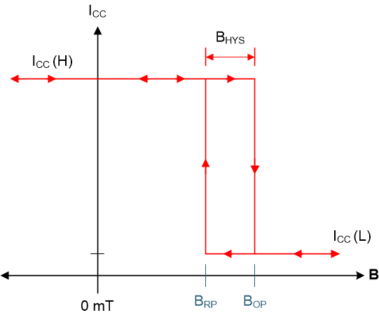
GUID-00E615D3-C973-4DBF-8DD4-90E65D44A5C3-low.gif Figure 8-3 Unipolar Functionality