JAJSHZ0A April   2013  – September 2019 TMP108

PRODUCTION DATA.  

  1. 特長
  2. アプリケーション
  3. 概要
    1.     Device Images
      1.      ブロック図
  4. 改訂履歴
  5. Pin Configuration and Functions
    1.     Pin Functions
  6. Specifications
    1. 6.1 Absolute Maximum Ratings
    2. 6.2 ESD Ratings
    3. 6.3 Recommended Operating Conditions
    4. 6.4 Thermal Information
    5. 6.5 Electrical Characteristics
    6. 6.6 Timing Diagrams
      1. 6.6.1 Two-Wire Timing Diagrams
    7. 6.7 Typical Characteristics
  7. Detailed Description
    1. 7.1 Overview
    2. 7.2 Functional Block Diagram
    3. 7.3 Feature Description
      1. 7.3.1 Serial Interface
      2. 7.3.2 Serial Bus Address
      3. 7.3.3 Bus Overview
      4. 7.3.4 Writing and Reading Operation
      5. 7.3.5 Slave Mode Operations
        1. 7.3.5.1 Slave Receiver Mode:
        2. 7.3.5.2 Slave Transmitter Mode:
      6. 7.3.6 SMBus Alert Function
      7. 7.3.7 General Call
      8. 7.3.8 High-Speed (Hs) Mode
      9. 7.3.9 Timeout Function
    4. 7.4 Device Functional Modes
      1. 7.4.1 Shutdown Mode (M1 = 0, M0 = 0)
      2. 7.4.2 One-Shot Mode (M1 = 0, M0 = 1)
      3. 7.4.3 Continuous Conversion Mode (M1 = 1)
    5. 7.5 Programming
      1. 7.5.1 Pointer Register
      2. 7.5.2 Temperature Register
      3. 7.5.3 Configuration Register
        1. 7.5.3.1 Hysteresis Control (HYS1 and HYS0)
        2. 7.5.3.2 Polarity (POL)
        3. 7.5.3.3 Thermostat Mode (TM)
        4. 7.5.3.4 Temperature Watchdog Flags (FL and FH)
        5. 7.5.3.5 Conversion Rate
      4. 7.5.4 High- and Low-Limit Registers
  8. Application and Implementation
    1. 8.1 Application Information
    2. 8.2 Typical Application
      1. 8.2.1 Design Requirements
      2. 8.2.2 Detailed Design Procedure
      3. 8.2.3 Application Curves
  9. Power Supply Recommendations
  10. 10Layout
    1. 10.1 Layout Guidelines
    2. 10.2 Layout Example
  11. 11デバイスおよびドキュメントのサポート
    1. 11.1 ドキュメントの更新通知を受け取る方法
    2. 11.2 サポート・リソース
    3. 11.3 商標
    4. 11.4 静電気放電に関する注意事項
    5. 11.5 Glossary
  12. 12メカニカル、パッケージ、および注文情報

パッケージ・オプション

メカニカル・データ(パッケージ|ピン)
サーマルパッド・メカニカル・データ
発注情報

Pointer Register

Figure 11 shows the internal register structure of the TMP108. Use the 8-bit pointer register to address a given data register. The pointer register uses the two LSBs (see Table 12) to identify which of the data registers respond to a read or write command. Table 3 identifies the bits of the pointer register byte. Table 4 describes the pointer address of the registers available in the TMP108. The power-up reset value of the P1 and P0 bits is 00.
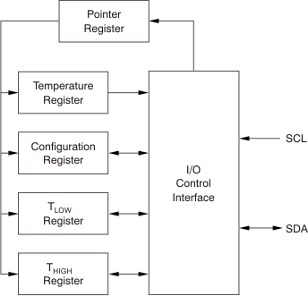
TMP108 ai_internal_reg_bos397.gifFigure 11. Internal Register Structure

Table 3. Pointer Register Byte

P7 P6 P5 P4 P3 P2 P1 P0
0 0 0 0 0 0 Register Bits

Table 4. Pointer Addresses

P1 P0 REGISTER
0 0 Temperature register (read only, default)
0 1 Configuration register (read/write)
1 0 TLOW register (read/write)
1 1 THIGH register (read/write)