SBOS760B November 2015 – April 2017 TMP275-Q1
PRODUCTION DATA.
- 1 Features
- 2 Applications
- 3 Description
- 4 Revision History
- 5 Pin Configuration and Functions
- 6 Specifications
- 7 Detailed Description
- 8 Application and Implementation
- 9 Power Supply Recommendations
- 10Layout
- 11Device and Documentation Support
- 12Mechanical, Packaging, and Orderable Information
パッケージ・オプション
メカニカル・データ(パッケージ|ピン)
サーマルパッド・メカニカル・データ
発注情報
8 Application and Implementation
NOTE
Information in the following applications sections is not part of the TI component specification, and TI does not warrant its accuracy or completeness. TI’s customers are responsible for determining suitability of components for their purposes. Customers should validate and test their design implementation to confirm system functionality.
8.1 Application Information
The TMP275-Q1 is a digital output temperature sensor with SMBus, two-wire, and I2C compatible interfaces. The device features three address pins (A0, A1, A2), allowing up to eight devices to be connected per bus. The TMP275-Q1 requires no external components for operation except for pullup resistors on SCL, SDA, and ALERT, although a 0.1-μF bypass capacitor is recommended. The TMP275-Q1 measures the printed circuit board (PCB) temperature of where the device is mounted. The sensing device of the TMP275-Q1 is the device itself. Thermal paths run through the package leads as well as the plastic package. The lower thermal resistance of metal causes the leads to provide the primary thermal path.
8.2 Typical Applications
8.2.1 Typical Connections of the TMP275-Q1
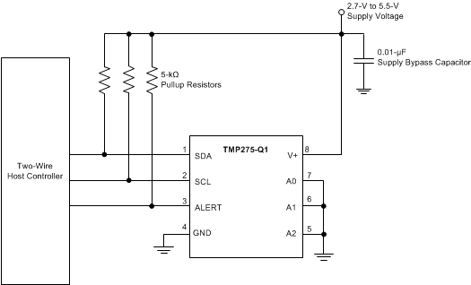
 Figure 13. Typical Connections of the TMP275-Q1 Schematic
8.2.1.1 Design Requirements
Figure 13 shows the TMP275-Q1 typical connections. The TMP275-Q1 device requires pullup resistors on the SCL, SDA, and ALERT pins. The recommended value for the pullup resistor is 5 kΩ. In some applications the pullup resistor can be lower or higher than 5 kΩ, but must not exceed 3 mA of current on the SCL and SDA pins and must not exceed 4 mA on the ALERT pin. If the resistors are missing, the SCL and SDA lines are always low (nearly 0 V) and the I2C bus does not work. A 0.1-μF bypass capacitor is recommended, as shown in Figure 13. The SCL, SDA, and ALERT lines can be pulled up to a supply that is equal to or higher than V+ through the pullup resistors.
The ALERT pin can be configured to respond to one of the two Alert functions available: comparator mode and interrupt mode. To configure one of eight different addresses on the bus, connect A0, A1, and A2 to either the GND or V+ pin. In the circuit shown in Figure 13, the comparator mode is selected and the address pins (A0, A1, A2) are connected to ground.
8.2.1.2 Detailed Design Procedure
Place the TMP275-Q1 device in close proximity to the heat source that must be monitored with a proper layout for good thermal coupling. This placement ensures that temperature changes are captured within the shortest possible time interval. To maintain accuracy in applications that require air or surface temperature measurement, take care to isolate the package and leads from ambient air temperature. A thermally-conductive adhesive is helpful in achieving accurate surface temperature measurement.
8.2.1.3 Application Curve
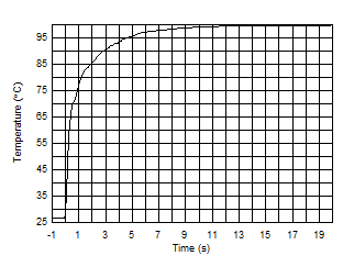
Figure 14 shows the step response of the TMP275-Q1 device to a submersion in an oil bath of 100ºC from room temperature (27ºC). The time-constant, or the time for the output to reach 63% of the input step, is 1.5 s. The time-constant result depends on the PCB where the TMP275-Q1 devices are mounted. For this test, the TMP275-Q1 device was soldered to a two-layer PCB that measured 0.375 inches × 0.437 inches.
 Figure 14. Temperature Step Response
8.2.2 Connecting Multiple Devices on a Single Bus
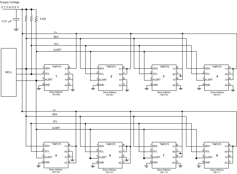
The TMP275-Q1 features three address pins, allowing up to eight devices to be connected per bus. When the TMP275-Q1 is operating in interrupt mode (TM = 1) , the ALERT pin of the TMP275-Q1 can be connected as an SMBus Alert signal. Figure 15 shows eight TMP275-Q1 devices connected to an MCU (master) using one single bus. Each device that exists as a slave on the SMBus has one unique 7-bit address; see Table 2 for the TMP275-Q1 address options. When a master senses that an Alert condition is present on the ALERT line, the master sends an SMBus Alert command (00011001) on the bus. If the ALERT pin of the TMP275-Q1 is active, the device acknowledges the SMBus Alert command and responds by returning its slave address on the SDA line. The eighth bit (LSB) of the slave address byte indicates if the temperature exceeding THIGH or falling below TLOW caused the ALERT condition. This bit is high if the temperature is greater than or equal to THIGH. This bit is low if the temperature is less than TLOW.
This application has eight devices connected to the bus. If multiple devices on the bus respond to the SMBus Alert command, arbitration during the slave address portion of the SMBus Alert command determines which device clears its ALERT status. If the TMP275-Q1 wins the arbitration, its ALERT pin becomes inactive at the completion of the SMBus Alert command. If the TMP275-Q1 loses the arbitration, its ALERT pin remains active.
NOTE
Make sure you device is configured to operate in interrupt mode to enable the SMBus feature.
 Figure 15. Connecting Multiple Devices on a Single Bus
8.2.3 Temperature Data Logger for Cold Chain Management Applications
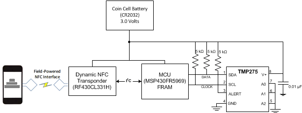
Cold chain management includes all of the means used to ensure a constant temperature for a product that is not heat stable from the time it is manufactured or farmed until the time it is used. This cold chain management includes industries such as food, retail, medical, and pharmaceutical. Figure 16 implements a cold chain monitoring system that measures temperature, then logs the sensor data to nonvolatile (FRAM) memory in the MCU. Figure 16 uses a near field communication (NFC) interface for wireless communication and is powered from a CR2032 coin cell battery with a focus on low power to maximize the battery lifetime.
The microcontroller communicates with all of the sensor devices through an I2C compatible interface. The MCU also communicates with the NFC transponder through this interface. An NFC-enabled smartphone can be used to send configurations to the application board. For a detailed design procedure and requirements of this application, see Ultralow Power Multi-sensor Data Logger with NFC Interface Reference Design.
 Figure 16. Temperature Data Logger