SBOS686A June 2013 – December 2014 TMP451
PRODUCTION DATA.
- 1 Features
- 2 Applications
- 3 Description
- 4 Revision History
- 5 Pin Configuration and Functions
- 6 Specifications
-
7 Detailed Description
- 7.1 Overview
- 7.2 Functional Block Diagram
- 7.3 Feature Description
- 7.4 Device Functional Modes
- 7.5 Programming
- 7.6
Register Map
- 7.6.1
Register Information
- 7.6.1.1 Pointer Register
- 7.6.1.2 Temperature Registers
- 7.6.1.3 Local Temperature High Byte Register (offset: Read = 00h; Write = N/A) [reset = 00h]
- 7.6.1.4 Remote Temperature High Byte Register (offset: Read = 01h; Write = N/A) [reset = 00h]
- 7.6.1.5 Status Register (offset: Read = 02h; Write = N/A) [reset = N/A]
- 7.6.1.6 Configuration Register (offset: Read = 03h; Write = 09h) [reset = 00h]
- 7.6.1.7 Conversion Rate Register (offset: Read = 04h; Write = 0Ah) [reset = 08h]
- 7.6.1.8 Local Temperature High Limit Register (offset: Read = 05h; Write = 0Bh) [reset = 55h]
- 7.6.1.9 Local Temperature Low Limit Register (offset: Read = 06h; Write = 0Ch) [reset = 00h]
- 7.6.1.10 Remote Temperature High Limit High Byte Register (offset: Read = 07h; Write = 0Dh) [reset = 55h]
- 7.6.1.11 Remote Temperature Low Limit High Byte Register (offset: Read = 08h; Write = 0Eh) [reset = 00h]
- 7.6.1.12 One-shot Start Register (offset: Read = N/A; Write = 0Fh) [reset = N/A]
- 7.6.1.13 Remote Temperature Low Byte Register (offset: Read = 10h; Write = N/A) [reset = 00h]
- 7.6.1.14 Remote Temperature Offset High Byte Register (offset: Read = 11h; Write = 11h) [reset = 00h]
- 7.6.1.15 Remote Temperature Offset Low Byte Register (offset: Read = 12h; Write = 12h) [reset = 00h]
- 7.6.1.16 Remote Temperature High Limit Low Byte Register (offset: Read = 13h; Write = 13h) [reset = 00h]
- 7.6.1.17 Remote Temperature Low Limit Low Byte Register (offset: Read = 14h; Write = 14h) [reset = 00h]
- 7.6.1.18 Local Temperature Low Byte Register (offset: Read = 15h; Write = N/A) [reset = 00h]
- 7.6.1.19 Remote Temperature THERM Limit Register (offset: Read = 19h; Write = 19h) [reset = 6C]
- 7.6.1.20 Local Temperature THERM Limit Register (offset: Read = 20h; Write = 20h) [reset = 55]
- 7.6.1.21 THERM Hysteresis Register (offset: Read = 21h; Write = 21h) [reset = 0Ah]
- 7.6.1.22 Consecutive ALERT Register (offset: Read = 22h; Write = 22h) [reset = 01h]
- 7.6.1.23 η-Factor Correction Register (offset: Read = 23h; Write = 23h) [reset = 00h]
- 7.6.1.24 Digital Filter Control Register (offset: Read = 24h; Write = 24h) [reset = 00h]
- 7.6.1.25 Manufacturer ID Register (offset: Read = FEh; Write = N/A) [reset = 55]
- 7.6.1
Register Information
- 8 Application and Implementation
- 9 Power Supply Recommendations
- 10Layout
- 11Device and Documentation Support
- 12Mechanical, Packaging, and Orderable Information
パッケージ・オプション
メカニカル・データ(パッケージ|ピン)
- DQF|8
サーマルパッド・メカニカル・データ
- DQF|8
発注情報
10 Layout
10.1 Layout Guidelines
Remote temperature sensing on the TMP451 device measures very small voltages using very low currents; therefore, noise at the device inputs must be minimized. Most applications using the TMP451 have high digital content, with several clocks and logic level transitions creating a noisy environment. Layout should adhere to the following guidelines:
- Place the TMP451 device as close to the remote junction sensor as possible.
- Route the D+ and D– traces next to each other and shield them from adjacent signals through the use of ground guard traces; see Figure 45. If a multilayer PCB is used, bury these traces between ground or V+ planes to shield them from extrinsic noise sources. 5 mil (0.127 mm) PCB traces are recommended.
- Minimize additional thermocouple junctions caused by copper-to-solder connections. If these junctions are used, make the same number and approximate locations of copper-to-solder connections in both the D+ and D– connections to cancel any thermocouple effects.
- Use a 0.1μF local bypass capacitor directly between the V+ and GND of the TMP451 device. For optimum measurement performance, minimize filter capacitance between D+ and D– to 1000 pF or less . This capacitance includes any cable capacitance between the remote temperature sensor and the TMP451 device.
- If the connection between the remote temperature sensor and the TMP451 device is less than 8-in (20,32 cm) long, use a twisted-wire pair connection. For lengths greater than 8 in, use a twisted, shielded pair with the shield grounded as close to the TMP451 device as possible. Leave the remote sensor connection end of the shield wire open to avoid ground loops and 60-Hz pickup.
- Thoroughly clean and remove all flux residue in and around the pins of the TMP451 device to avoid temperature offset readings as a result of leakage paths between D+ and GND, or between D+ and V+.
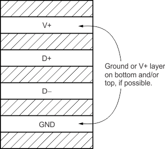
Use minimum 5-mil (0.127 mm) traces with 5-mil spacing.
Figure 45. Suggested PCB Layer Cross-Section
10.2 Layout Example
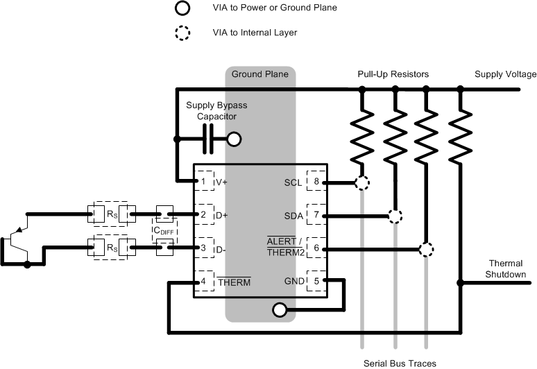 Figure 46. TMP451 Layout Example