JAJSLK1A october 2022 – march 2023 TMUX7201 , TMUX7202
PRODUCTION DATA
- 1 特長
- 2 アプリケーション
- 3 概要
- 4 Revision History
- 5 Pin Configuration and Functions
-
6 Specifications
- 6.1 Absolute Maximum Ratings
- 6.2 ESD Ratings
- 6.3 Thermal Information
- 6.4 Recommended Operating Conditions
- 6.5 Source or Drain Continuous Current
- 6.6 ±15 V Dual Supply: Electrical Characteristics
- 6.7 ±15 V Dual Supply: Switching Characteristics
- 6.8 ±20 V Dual Supply: Electrical Characteristics
- 6.9 ±20 V Dual Supply: Switching Characteristics
- 6.10 44 V Single Supply: Electrical Characteristics
- 6.11 44 V Single Supply: Switching Characteristics
- 6.12 12 V Single Supply: Electrical Characteristics
- 6.13 12 V Single Supply: Switching Characteristics
- 6.14 Typical Characteristics
- 7 Parameter Measurement Information
- 8 Detailed Description
- 9 Application and Implementation
- 10Device and Documentation Support
- 11Mechanical, Packaging, and Orderable Information
パッケージ・オプション
デバイスごとのパッケージ図は、PDF版データシートをご参照ください。
メカニカル・データ(パッケージ|ピン)
- RQX|8
サーマルパッド・メカニカル・データ
発注情報
8.3.7 Ultra-Low Charge Injection
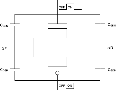
Figure 8-1 shows how the TMUX720x devices have a transmission gate topology. Any mismatch in the stray capacitance associated with the NMOS and PMOS causes an output level change whenever the switch is opened or closed.
 Figure 8-1 Transmission Gate Topology
The TMUX720x contains specialized architecture to reduce charge injection on the Drain (Dx). To further reduce charge injection in a sensitive application, a compensation capacitor (Cp) can be added on the Source (S). By design, the excess charge from the switch transition will be pushed into the compensation capacitor on the Source (S) instead of the Drain (D). As a general rule, Cp should be 20x larger than the equivalent load capacitance on the Drain (D). Figure 8-2 shows charge injection variation with different compensation capacitors on the Source side. This plot was captured on the TMUX7219 as part of the TMUX72xx family with a 100 pF load capacitance.
 Figure 8-2 Charge Injection Compensation