JAJSN29B october 2021 – march 2023 TMUX8211 , TMUX8212 , TMUX8213
PRODUCTION DATA
- 1 特長
- 2 アプリケーション
- 3 概要
- 4 Revision History
- 5 Device Comparison Table
- 6 Pin Configuration and Functions
-
7 Specifications
- 7.1 Absolute Maximum Ratings: TMUX821x Devices
- 7.2 ESD Ratings
- 7.3 Recommended Operating Conditions: TMUX821x Devices
- 7.4 ソースまたはドレイン連続電流
- 7.5 ドレイン・パルス電流のソース
- 7.6 Thermal Information
- 7.7 Electrical Characteristics (Global): TMUX821x Devices
- 7.8 Electrical Characteristics (±15-V Dual Supply)
- 7.9 Electrical Characteristics (±36-V Dual Supply)
- 7.10 Electrical Characteristics (±50-V Dual Supply)
- 7.11 Electrical Characteristics (72-V Single Supply)
- 7.12 Electrical Characteristics (100-V Single Supply)
- 7.13 Switching Characteristics: TMUX821x Devices
- 7.14 Typical Characteristics
- 8 Parameter Measurement Information
- 9 Detailed Description
- 10Application and Implementation
- 11Power Supply Recommendations
- 12Layout
- 13Device and Documentation Support
- 14Mechanical, Packaging, and Orderable Information
パッケージ・オプション
メカニカル・データ(パッケージ|ピン)
サーマルパッド・メカニカル・データ
- RUM|16
発注情報
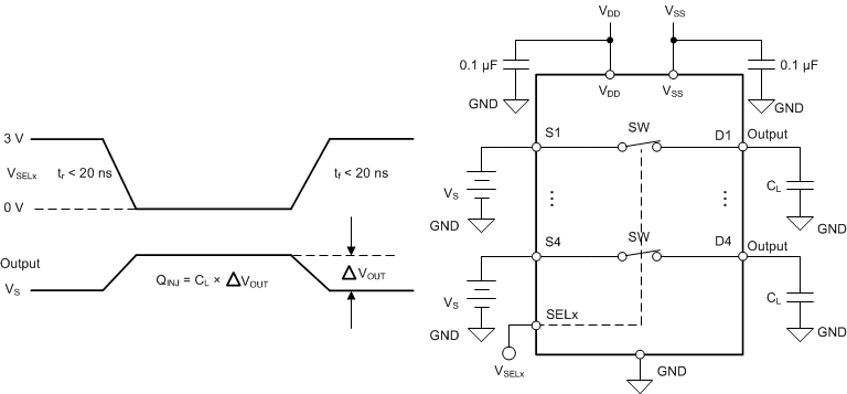
8.5 Charge Injection
Charge injection is a measure of the glitch impulse transferred from the digital input to the analog output during switching, and is denoted by the symbol QINJ. Figure 8-5 shows the setup used to measure charge injection from the source to drain.
 Figure 8-5 Charge-Injection Measurement
Setup