SLOS498B September 2006 – September 2015 TPA2006D1
PRODUCTION DATA.
- 1 Features
- 2 Applications
- 3 Description
- 4 Revision History
- 5 Device Comparison Table
- 6 Pin Configuration and Functions
- 7 Specifications
- 8 Parameter Measurement Information
- 9 Detailed Description
- 10Application and Implementation
- 11Power Supply Recommendations
- 12Layout
- 13Device and Documentation Support
- 14Mechanical, Packaging, and Orderable Information
パッケージ・オプション
メカニカル・データ(パッケージ|ピン)
- DRB|8
サーマルパッド・メカニカル・データ
- DRB|8
発注情報
9 Detailed Description
9.1 Overview
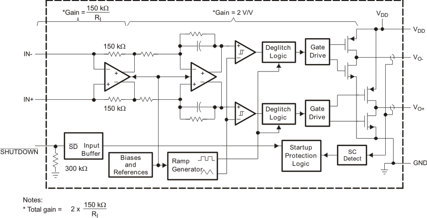
The TPA2006D1 device is a high-efficiency, filter-free, Class-D audio amplifier capable of delivering up to 1.45 W into 8-Ω loads with 5-V power supply. Shutdown control is fully compatible with 1.8-V logic levels.
The fully differential design of this amplifier avoids the usage of bypass capacitors and the improved CMRR eliminates the usage of input coupling capacitors. This makes the device size a perfect choice for small, portable applications as only three external components are required.
The advanced modulation used in the TPA2006D1 device PWM output stage eliminates the need for an output filter.
9.2 Functional Block Diagram
9.3 Feature Description
9.3.1 Fully Differential Amplifier
The TPA2006D1 device is a fully differential amplifier with differential inputs and outputs. The fully differential amplifier consists of a differential amplifier and a common-mode amplifier. The differential amplifier ensures that the amplifier outputs a differential voltage on the output that is equal to the differential input times the gain. The common-mode feedback ensures that the common-mode voltage at the output is biased around VDD/2 regardless of the common-mode voltage at the input. The fully differential TPA2006D1 device can still be used with a single-ended input; however, the TPA2006D1 device must be used with differential inputs when in a noisy environment, like a wireless handset, to ensure maximum noise rejection.
9.3.1.1 Advantages of Fully Differential Amplifiers
- Input-coupling capacitors not required:
- The fully differential amplifier allows the inputs to be biased at voltage other than mid-supply. For example, if a codec has a mid-supply lower than the mid-supply of the TPA2006D1 device, the common-mode feedback circuit will adjust, and the TPA2006D1 device outputs will still be biased at mid-supply of the TPA2006D1 device. The inputs of the TPA2006D1 device can be biased from 0.5 V to VDD – 0.8 V. If the inputs are biased outside of that range, input-coupling capacitors are required.
- Mid-supply bypass capacitor, C(BYPASS), not required:
- The fully differential amplifier does not require a bypass capacitor. This is because any shift in the midsupply affects both positive and negative channels equally and cancels at the differential output.
- Better RF-immunity:
- GSM handsets save power by turning on and shutting off the RF transmitter at a rate of 217 Hz. The transmitted signal is picked-up on input and output traces. The fully differential amplifier cancels the signal much better than the typical audio amplifier.
9.3.2 Efficiency and Thermal Information
The maximum ambient temperature depends on the heat-sinking ability of the PCB system. The derating factor for the DRB package is shown in the dissipation rating table. Converting this to θJA:

Given θJA of 45.9°C/W, the maximum allowable junction temperature of 125°C, and the maximum internal dissipation of 0.2 W (Po = 1.45 W, 8-Ω load, 5-V supply, from Figure 3), the maximum ambient temperature can be calculated with Equation 2.

Equation 2 shows that the calculated maximum ambient temperature is 115.8°C at maximum power dissipation with a 5-V supply and 8-Ω a load, see Figure 3. The TPA2006D1 device is designed with thermal protection that turns the device off when the junction temperature surpasses 150°C to prevent damage to the device.
9.3.3 Eliminating the Output Filter With the TPA2006D1 Device
This section focuses on why the user can eliminate the output filter with the TPA2006D1 device.
9.3.3.1 Effect on Audio
The class-D amplifier outputs a pulse-width modulated (PWM) square wave, which is the sum of the switching waveform and the amplified input audio signal. The human ear acts as a band-pass filter such that only the frequencies between approximately 20 Hz and 20 kHz are passed. The switching frequency components are much greater than 20 kHz, so the only signal heard is the amplified input audio signal.
9.3.3.2 Traditional Class-D Modulation Scheme
The traditional class-D modulation scheme, which is used in the TPA005Dxx family, has a differential output where each output is 180 degrees out of phase and changes from ground to the supply voltage, VDD. Therefore, the differential pre-filtered output varies between positive and negative VDD, where filtered 50% duty cycle yields 0 volts across the load. The traditional class-D modulation scheme with voltage and current waveforms is shown in Figure 28. Note that even at an average of 0 volts across the load (50% duty cycle), the current to the load is high causing a high loss and thus causing a high supply current.
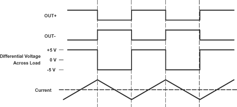 Figure 28. Traditional Class-D Modulation Scheme's Output Voltage and Current Waveforms into an Inductive Load With no Input
9.3.3.3 TPA2006D1 Device Modulation Scheme
The TPA2006D1 device uses a modulation scheme that still has each output switching from 0 to the supply voltage. However, OUT+ and OUT– are now in phase with each other with no input. The duty cycle of OUT+ is greater than 50% and OUT– is less than 50% for positive voltages. The duty cycle of OUT+ is less than 50% and OUT– is greater than 50% for negative voltages. The voltage across the load sits at 0 volts throughout most of the switching period greatly reducing the switching current, which reduces any I2R losses in the load.
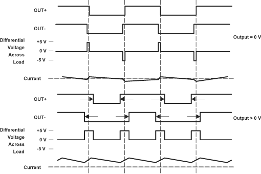 Figure 29. The TPA2006D1 Device Output Voltage and Current Waveforms into an Inductive Load
9.3.3.4 Efficiency: Why A Filter is Needed With the Traditional Class-D Modulation Scheme
The main reason that the traditional class-D amplifier needs an output filter is that the switching waveform results in maximum current flow. This causes more loss in the load, which causes lower efficiency. The ripple current is large for the traditional modulation scheme because the ripple current is proportional to voltage multiplied by the time at that voltage. The differential voltage swing is 2 × VDD and the time at each voltage is half the period for the traditional modulation scheme. An ideal LC filter is needed to store the ripple current from each half cycle for the next half cycle, while any resistance causes power dissipation. The speaker is both resistive and reactive, whereas an LC filter is almost purely reactive.
The TPA2006D1 device modulation scheme has little loss in the load without a filter because the pulses are short and the change in voltage is VDD instead of 2 × VDD. As the output power increases, the pulses widen making the ripple current larger. Ripple current could be filtered with an LC filter for increased efficiency, but for most applications the filter is not needed.
An LC filter with a cutoff frequency less than the class-D switching frequency allows the switching current to flow through the filter instead of the load. The filter has less resistance than the speaker that results in less power dissipated, which increases efficiency.
9.3.3.5 Effects of Applying a Square Wave into a Speaker
If the amplitude of a square wave is high enough and the frequency of the square wave is within the bandwidth of the speaker, a square wave could cause the voice coil to jump out of the air gap and/or scar the voice coil. A 250-kHz switching frequency, however, is not significant because the speaker cone movement is proportional to 1/f2 for frequencies beyond the audio band. Therefore, the amount of cone movement at the switching frequency is small. However, damage could occur to the speaker if the voice coil is not designed to handle the additional power. To size the speaker for added power, the ripple current dissipated in the load needs to be calculated by subtracting the theoretical supplied power, PSUP THEORETICAL, from the actual supply power, PSUP, at maximum output power, POUT. The switching power dissipated in the speaker is the inverse of the measured efficiency, ηMEASURED, minus the theoretical efficiency, ηTHEORETICAL.


The maximum efficiency of the TPA2006D1 device with a 3.6-V supply and an 8-Ω load is 86% from Equation 6. Using Equation 5 with the efficiency at maximum power (84%), we see that there is an additional 17 mW dissipated in the speaker. The added power dissipated in the speaker is not an issue as long as it is taken into account when choosing the speaker.
9.3.3.6 When to Use an Output Filter
Design the TPA2006D1 device without an output filter if the traces from amplifier to speaker are short. The TPA2006D1 device passed FCC and CE radiated emissions with no shielding with speaker trace wires 100 mm long or less. Wireless handsets and PDAs are great applications for class-D without a filter.
A ferrite bead filter can often be used if the design is failing radiated emissions without an LC filter, and the frequency sensitive circuit is greater than 1 MHz. This is good for circuits that just have to pass FCC and CE because FCC and CE only test radiated emissions greater than 30 MHz. If choosing a ferrite bead, choose one with high impedance at high frequencies, but low impedance at low frequencies.
Use an LC output filter if there are low frequency (< 1 MHz) EMI sensitive circuits and/or there are long leads from amplifier to speaker.
Figure 30 and Figure 31 show typical ferrite bead and LC output filters.
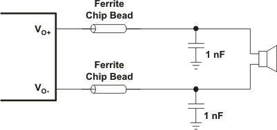 Figure 30. Typical Ferrite Chip Bead Filter (Chip Bead Example: NEC/Tokin: N2012ZPS121)
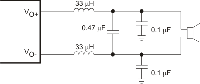 Figure 31. Typical LC Output Filter, Cutoff Frequency of 27 kHz
9.3.4 Thermal and Short-Circuit Protection
The TPA2006D1 device features thermal and short- circuit protection. When the protection circuit is triggered, the device will enter in shutdown mode, setting the outputs of the device into High Impedance. Thermal protection turns the device off when the junction temperature surpasses 150°C to prevent damage to the device.
9.4 Device Functional Modes
9.4.1 Summing Input Signals with the TPA2006D1 Device
Most wireless phones or PDAs need to sum signals at the audio power amplifier or just have two signal sources that need separate gain. The TPA2006D1 device makes it easy to sum signals or use separate signal sources with different gains. Many phones now use the same speaker for the earpiece and ringer, where the wireless phone would require a much lower gain for the phone earpiece than for the ringer. PDAs and phones that have stereo headphones require summing of the right and left channels to output the stereo signal to the mono speaker.
9.4.1.1 Summing Two Differential Input Signals
Two extra resistors are needed for summing differential signals (a total of 5 components). The gain for each input source can be set independently (see Equation 7 and Equation 8, and Figure 32).


If summing left and right inputs with a gain of 1 V/V, use RI1 = RI2 = 300 kΩ.
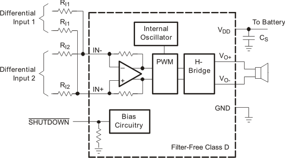 Figure 32. Application Schematic With TPA2006D1 Device Summing Two Differential Inputs
9.4.1.2 Summing a Differential Input Signal and a Single-Ended Input Signal
Figure 33 shows how to sum a differential input signal and a single-ended input signal. Ground noise can couple in through IN+ with this method. It is better to use differential inputs. The corner frequency of the single-ended input is set by CI2, shown in Equation 11. To assure that each input is balanced, the single-ended input must be driven by a low-impedance source even if the input is not in use


If summing a ring tone and a phone signal, the phone signal must use a differential input signal while the ring tone might be limited to a single-ended signal.
The high pass corner frequency of the single-ended input is set by CI2. If the desired corner frequency is less than 20 Hz:


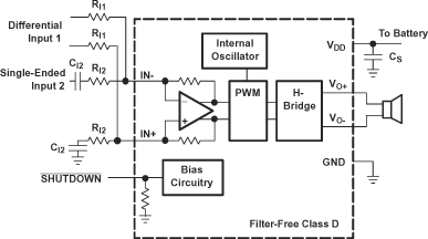 Figure 33. Application Schematic With TPA2006D1 Device Summing Differential Input and Single-Ended Input Signals
9.4.1.3 Summing Two Single-Ended Input Signals
Four resistors and three capacitors are needed for summing single-ended input signals. The gain and corner frequencies (fc1 and fc2) for each input source can be set independently (see Equation 14 through Equation 17, and Figure 34). Resistor, RP, and capacitor, CP, are needed on the IN+ terminal to match the impedance on the IN– terminal. The single-ended inputs must be driven by low impedance sources even if one of the inputs is not outputting an AC signal.


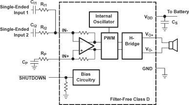 Figure 34. Application Schematic With TPA2006D1 Device Summing Two Single-Ended Inputs
9.4.2 Shutdown Mode
The TPA2006D1 device can be put in shutdown mode when asserting SHUTDOWN pin to a logic LOW. While in shutdown mode, the device output stage is turned off and set into High Impedance, making the current consumption very low. The device exits shutdown mode when a HIGH logic level is applied to SHUTDOWN pin.