SLOS524E June 2008 – May 2016 TPA2016D2
PRODUCTION DATA.
- 1 Features
- 2 Applications
- 3 Description
- 4 Revision History
- 5 Device Comparison Table
- 6 Pin Configuration and Functions
- 7 Specifications
- 8 Parameter Measurement Information
- 9 Detailed Description
- 10Application and Implementation
- 11Power Supply Recommendations
- 12Layout
- 13Device and Documentation Support
- 14Mechanical, Packaging, and Orderable Information
パッケージ・オプション
メカニカル・データ(パッケージ|ピン)
サーマルパッド・メカニカル・データ
- RTJ|20
発注情報
7 Specifications
7.1 Absolute Maximum Ratings
over operating free-air temperature range (unless otherwise noted).(1)| MIN | MAX | UNIT | |||
|---|---|---|---|---|---|
| VDD | Supply voltage | AVDD, PVDDR, PVDDL | –0.3 | 6 | V |
| Input voltage | SDZ, INR+, INR–, INL+, INL– | –0.3 | VDD + 0.3 | V | |
| SDA, SCL | –0.3 | 6 | |||
| Continuous total power dissipation | See Dissipation Ratings | ||||
| TA | Operating free-air temperature | –40 | 85 | °C | |
| TJ | Operating junction temperature | –40 | 150 | °C | |
| RLOAD | Minimum load resistance | 3.2 | Ω | ||
| Tstg | Storage temperature | –65 | 150 | °C | |
(1) Stresses beyond those listed under Absolute Maximum Ratings may cause permanent damage to the device. These are stress ratings only, which do not imply functional operation of the device at these or any other conditions beyond those indicated under Recommended Operating Conditions. Exposure to absolute-maximum-rated conditions for extended periods may affect device reliability.
7.2 ESD Ratings
| VALUE | UNIT | |||
|---|---|---|---|---|
| V(ESD) | Electrostatic discharge | Human-body model (HBM), per ANSI/ESDA/JEDEC JS-001(1) | ±2000 | V |
| Charged-device model (CDM), per JEDEC specification JESD22-C101(2) | ±500 | |||
(1) JEDEC document JEP155 states that 500-V HBM allows safe manufacturing with a standard ESD control process.
(2) JEDEC document JEP157 states that 250-V CDM allows safe manufacturing with a standard ESD control process.
7.3 Recommended Operating Conditions
| MIN | MAX | UNIT | |||
|---|---|---|---|---|---|
| VDD | Supply voltage | AVDD, PVDDR, PVDDL | 2.5 | 5.5 | V |
| VIH | High-level input voltage | SDZ, SDA, SCL | 1.3 | V | |
| VIL | Low-level input voltage | SDZ, SDA, SCL | 0.6 | V | |
| TA | Operating free-air temperature | –40 | +85 | °C | |
7.4 Thermal Information
| THERMAL METRIC(1) | TPA2016D2 | UNIT | ||
|---|---|---|---|---|
| YZH (DSBGA) | RTJ (QFN) | |||
| 16 PINS | 20 PINS | |||
| RθJA | Junction-to-ambient thermal resistance | 71 | 33.3 | °C/W |
| RθJC(top) | Junction-to-case (top) thermal resistance | 0.4 | 22.5 | °C/W |
| RθJB | Junction-to-board thermal resistance | 14.4 | 9.6 | °C/W |
| ψJT | Junction-to-top characterization parameter | 1.9 | 0.2 | °C/W |
| ψJB | Junction-to-board characterization parameter | 13.6 | 9.6 | °C/W |
| RθJC(bot) | Junction-to-case (bottom) thermal resistance | — | 2.4 | °C/W |
(1) For more information about traditional and new thermal metrics, see the Semiconductor and IC Package Thermal Metrics application report, SPRA953.
7.5 Electrical Characteristics
at TA = 25°C, VDD = 3.6 V, SDZ = 1.3 V, and RL = 8 Ω + 33 μH (unless otherwise noted).7.6 I2C Timing Requirements
For I2C Interface Signals Over Recommended Operating Conditions (unless otherwise noted)| MIN | TYP | MAX | UNIT | |||
|---|---|---|---|---|---|---|
| fSCL | Frequency, SCL | No wait states | 400 | kHz | ||
| tW(H) | Pulse duration, SCL high | 0.6 | μs | |||
| tW(L) | Pulse duration, SCL low | 1.3 | μs | |||
| tSU(1) | Setup time, SDA to SCL | 100 | ns | |||
| th1 | Hold time, SCL to SDA | 10 | ns | |||
| t(buf) | Bus free time between stop and start condition | 1.3 | μs | |||
| tSU2 | Setup time, SCL to start condition | 0.6 | μs | |||
| th2 | Hold time, start condition to SCL | 0.6 | μs | |||
| tSU3 | Setup time, SCL to stop condition | 0.6 | μs | |||
7.7 Dissipation Ratings
| PACKAGE(1) | TA ≤ 25°C | DERATING FACTOR | TA = 70°C | TA = 85°C |
|---|---|---|---|---|
| 16-ball DSBGA | 1.25 W | 10 mW/°C | 0.8 W | 0.65 W |
| 20–pin QFN | 5.2 W | 41.6 mW/°C | 3.12 W | 2.7 W |
(1) Dissipations ratings are for a 2-side, 2-plane PCB.
7.8 Operating Characteristics
at TA = 25°C, VDD = 3.6V, SDZ = 1.3 V, RL = 8 Ω +33 μH, and AV = 6 dB (unless otherwise noted).| MIN | TYP | MAX | UNIT | |||
|---|---|---|---|---|---|---|
| kSVR | Power-supply ripple rejection ratio | VDD = 3.6 Vdc with ac of 200 mVPP at 217 Hz | –68 | dB | ||
| THD+N | Total harmonic distortion + noise | faud_in = 1 kHz; PO = 550 mW; VDD = 3.6 V | 0.1% | |||
| faud_in = 1 kHz; PO = 1 W; VDD = 5 V | 0.1% | |||||
| faud_in = 1 kHz; PO = 630 mW; VDD = 3.6 V | 1% | |||||
| faud_in = 1 kHz; PO = 1.4 W; VDD = 5 V | 1% | |||||
| NfonF | Output integrated noise | Av = 6 dB | 44 | μV | ||
| NfoA | Output integrated noise | Av = 6 dB floor, A-weighted | 33 | μV | ||
| FR | Frequency response | Av = 6 dB | 20 | 20000 | Hz | |
| Pomax | Maximum output power | THD+N = 10%, VDD = 5 V, RL = 8 Ω | 1.72 | W | ||
| THD+N = 10%, VDD = 3.6 V, RL = 8 Ω | 750 | mW | ||||
| THD+N = 10%, VDD = 5 V, RL = 4 Ω | 2.8 | W | ||||
| THD+N = 10% , VDD = 3.6 V, RL = 4 Ω | 1.5 | mW | ||||
| η | Efficiency | THD+N = 1%, VDD = 3.6 V, RL = 8 Ω, PO= 0.63 W | 90% | |||
| THD+N = 1%, VDD = 5 V, RL = 8 Ω, PO = 1.4 W | 90% | |||||
 Figure 1. SCL and SDA Timing
 Figure 2. Start and Stop Conditions Timing
7.9 Typical Characteristics
with C(DECOUPLE) = 1 μF, CI = 1 µF.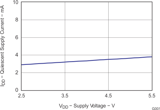 Figure 3. Quiescent Supply Current vs Supply Voltage
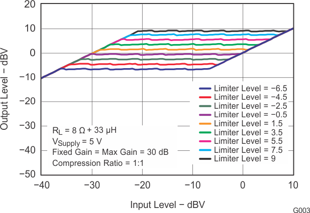 Figure 5. Output Level vs Input Level With Limiter Enabled
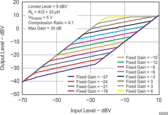 Figure 7. Output Level vs Input Level With 4:1 Compression
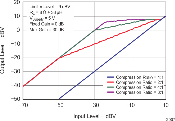 Figure 9. Output Level vs Input Level
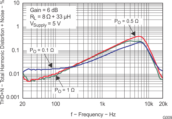 Figure 11. Total Harmonic Distortion + Noise vs Frequency
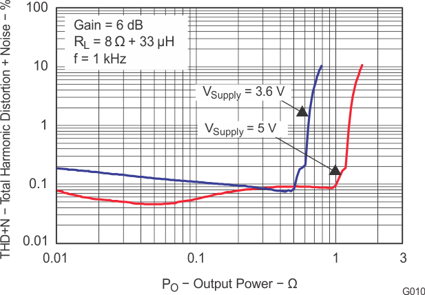 Figure 13. Total Harmonic Distortion + Noise vs Output Power
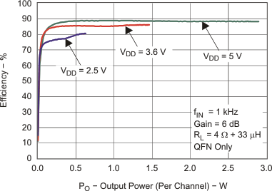
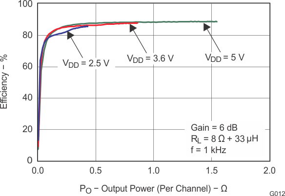 Figure 15. Efficiency vs Output Power (Per Channel)
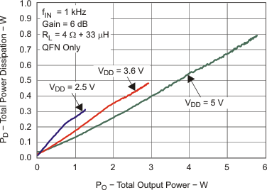
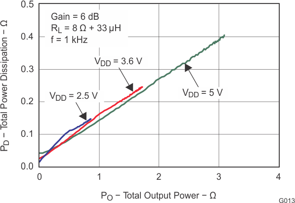 Figure 17. Total Power Dissipation vs Total Output Power
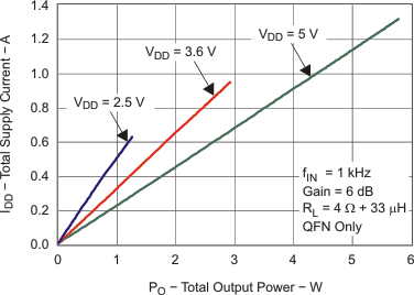
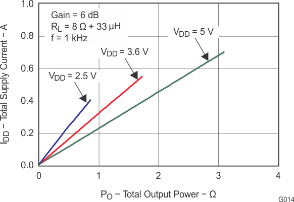 Figure 19. Total Supply Current vs Total Output Power
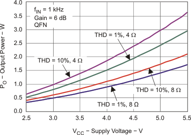
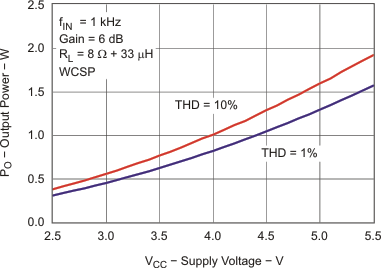 Figure 21. Output Power vs Supply Voltage
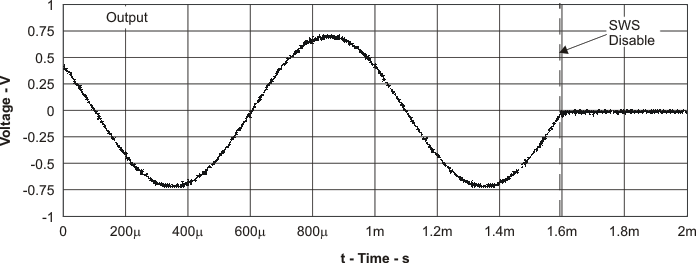 Figure 23. Shutdown Time
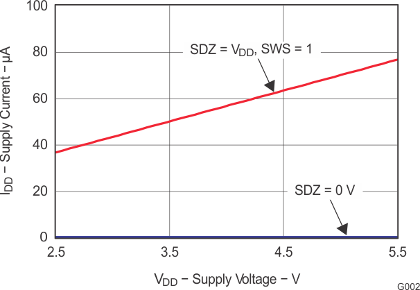 Figure 4. Supply Current vs Supply Voltage in Shutdown
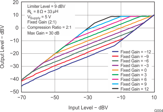 Figure 6. Output Level vs Input Level With 2:1 Compression
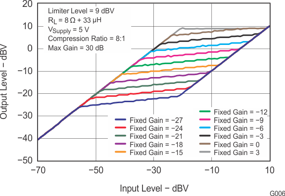 Figure 8. Output Level vs Input Level With 8:1 Compression
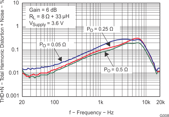 Figure 10. Total Harmonic Distortion + Noise vs Frequency
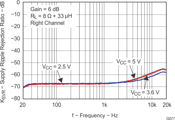 Figure 12. Supply Ripple Rejection Ratio
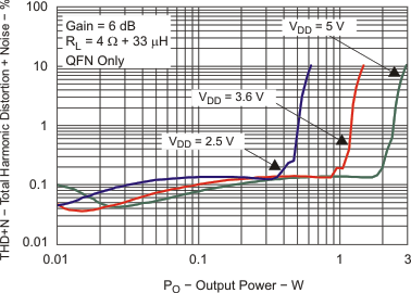 Figure 14. Total Harmonic Distortion + Noise vs Output Power
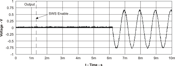 Figure 24. Start-Up Time
