SLOS794B September 2012 – September 2015 TPA3110D2-Q1
PRODUCTION DATA.
- 1 Features
- 2 Applications
- 3 Description
- 4 Revision History
- 5 Pin Configuration and Functions
- 6 Specifications
- 7 Detailed Description
-
8 Application and Implementation
- 8.1 Application Information
- 8.2
Typical Application
- 8.2.1 Design Requirements
- 8.2.2
Detailed Design Procedure
- 8.2.2.1 TPA3110D2-Q1 Modulation Scheme
- 8.2.2.2 Ferrite Bead Filter Considerations
- 8.2.2.3 Efficiency: LC Filter Required With the Traditional Class-D Modulation Scheme
- 8.2.2.4 When to Use an Output Filter for EMI Suppression
- 8.2.2.5 Input Resistance
- 8.2.2.6 Input Capacitor, CI
- 8.2.2.7 BSN and BSP Capacitors
- 8.2.2.8 Differential Inputs
- 8.2.2.9 Using Low-ESR Capacitors
- 8.2.3 Application Curve
- 9 Power Supply Recommendations
- 10Layout
- 11Device and Documentation Support
- 12Mechanical, Packaging, and Orderable Information
パッケージ・オプション
メカニカル・データ(パッケージ|ピン)
- PWP|28
サーマルパッド・メカニカル・データ
- PWP|28
発注情報
7 Detailed Description
7.1 Overview
The TPA3110D2-Q1 is AEC-Q100 qualified with a temperature grade 1 (-40°C to 125°C), HBM ESD classification level H2, and CDM ESD classification level C2. This automotive audio amplifier also features several protection mechanisms as follows:
- DC Current Detection
- The TPA3110D2-Q1 protects speakers from DC current by reporting a fault on the FAULT pin and turning the amplifier outputs to a Hi-Z state when a DC current is detected. The PVCC supply must be cycled to clear this fault.
- Short-Circuit Protection and Automatic Recovery
- The TPA3110D2-Q1 has short circuit protection from the output pins to VCC, GND, or to each other. If a short circuit is detected, it will be reported on the FAULT pin and the amplifier outputs will be switched to a Hi-Z state. The fault can be cleared by cycling the SD pin.
- Thermal Protection
- When the die temperature exceeds 150°C (±15°C) the device enters the shutdown state and the amplifier outputs are disabled. The TPA3110D2-Q1 recovers automatically when the temperature decreases by 15°C
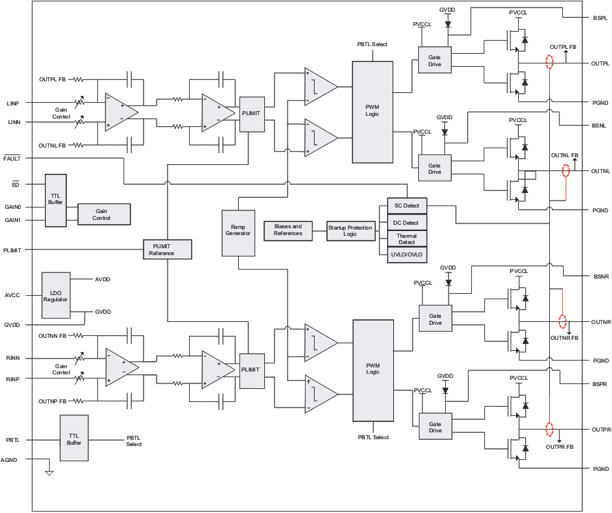
7.2 Functional Block Diagram

7.3 Feature Description
7.3.1 DC Detect
TPA3110D2-Q1 has circuitry which protects the speakers from DC current which might occur due to defective capacitors on the input or shorts on the printed circuit board at the inputs. A DC detect fault is reported on the FAULT pin as a low state. The DC detect fault also causes the amplifier to shut down by changing the state of the outputs to Hi-Z. To clear the DC detect it is necessary to cycle the PVCC supply. Cycling SD does NOT clear a DC detect fault.
A DC detect fault is issued when the output differential duty-cycle of either channel exceeds 14% (for example, 57%, –43%) for more than 420 msec at the same polarity. This feature protects the speaker from large DC currents or AC currents less than 2 Hz. To avoid nuisance faults due to the DC detect circuit, hold the SD pin low at power-up until the signals at the inputs are stable. Also, take care to match the impedance seen at the positive and negative inputs to avoid nuisance DC detect faults.
The minimum differential input voltages required to trigger the DC detect are shown in Table 1. The inputs must remain at or above the voltage listed in the table for more than 420 msec to trigger the DC detect.
Table 1. DC Detect Threshold
| AV (dB) | VIN (mV, Differential) |
|---|---|
| 20 | 112 |
| 26 | 56 |
| 32 | 28 |
| 36 | 17 |
7.3.2 Short-Circuit Protection and Automatic Recovery Feature
TPA3110D2-Q1 has protection from overcurrent conditions caused by a short circuit on the output stage. The short-circuit protection fault is reported on the FAULT pin as a low state. The amplifier outputs are switched to a Hi-Z state when the short-circuit protection latch is engaged. The latch can be cleared by cycling the SD pin through the low state.
If automatic recovery from the short-circuit protection latch is desired, connect the FAULT pin directly to the SD pin. This allows the FAULT pin function to automatically drive the SD pin low, which clears the short-circuit protection latch.
7.3.3 Thermal Protection
Thermal protection on the TPA3110D2-Q1 prevents damage to the device when the internal die temperature exceeds 150°C. There is a ±15°C tolerance on this trip point from device to device. Once the die temperature exceeds the thermal set point, the device enters into the shutdown state and the outputs are disabled. This is not a latched fault. The thermal fault is cleared once the temperature of the die is reduced by 15°C. The device begins normal operation at this point with no external system interaction.
Thermal protection faults are NOT reported on the FAULT terminal.
7.3.4 GVDD Supply
The GVDD supply is used to power the gates of the output full bridge transistors. It can also be used to supply the PLIMIT voltage divider circuit. Add a 1-μF capacitor to ground at this pin.
7.4 Device Functional Modes
7.4.1 PBTL Select
Use the PBTL pin to select between PBTL mode when held high or BTL mode when held low. Connect the speaker between the right and left outputs, with the positive and negative output from each channel tied together.
7.4.2 Gain Setting Through GAIN0 and GAIN1 Inputs
The gain of the TPA3110D2-Q1 is set to one of four options by the state of the GAIN0 and GAIN1 pins. Changing the gain setting also changes the input impedance of the TPA3110D2-Q1.
Refer to Table 2 for a list of the gain settings.
Table 2. Gain Setting
| GAIN1 | GAIN0 | AMPLIFIER GAIN (dB) | INPUT IMPEDANCE (kΩ) |
|---|---|---|---|
| TYP | TYP | ||
| 0 | 0 | 20 | 60 |
| 0 | 1 | 26 | 30 |
| 1 | 0 | 32 | 15 |
| 1 | 1 | 36 | 9 |
7.4.3 SD Operation
The SD pin can be used to enter the shutdown mode which mutes the amplifier and causes the TPA3110D2-Q1 to enter a low-current state. This mode can also be triggered to improve power-off pop performance.
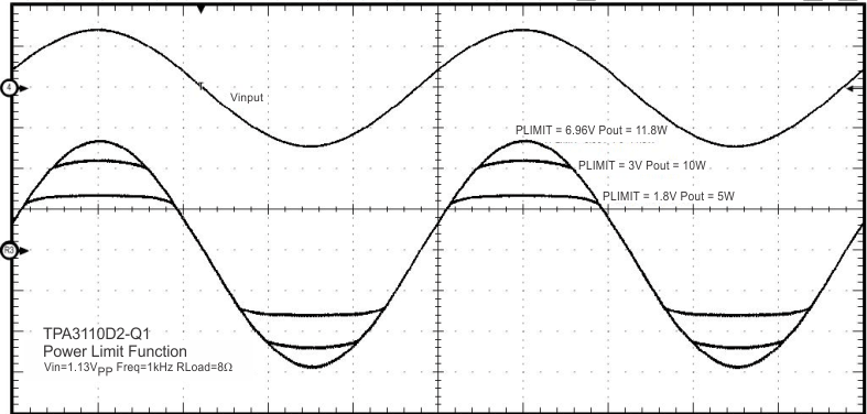
7.4.4 PLIMIT
The PLIMIT pin limits the output peak-to-peak voltage based on the voltage supplied to the PLIMIT pin. The peak output voltage is limited to four times the voltage at the PLIMIT pin.
 Figure 35. PLIMIT Circuit Operation
The PLIMIT circuit sets a limit on the output peak-to-peak voltage. The limiting is done by limiting the duty cycle to fixed maximum value. This limit can be thought of as a virtual voltage rail which is lower than the supply connected to PVCC. This virtual rail is four times the voltage at the PLIMIT pin. This output voltage can be used to calculate the maximum output power for a given maximum input voltage and speaker impedance.

Where:
RS is the total series resistance including RDS(on), and any resistance in the output filter.
RL is the load resistance.
VP is the peak amplitude of the output possible within the supply rail.
VP = 4 × PLIMIT voltage if PLIMIT < 4 × VP
POUT (10%THD) = 1.25 × POUT (unclipped)
Table 3. PLIMIT Typical Operation
| TEST CONDITIONS | PLIMIT VOLTAGE | OUTPUT POWER (W) | Output Voltage Amplitude (VP-P) |
|---|---|---|---|
| PVCC = 24 V, VIN = 1 VRMS, RL = 8 Ω, Gain = 26 dB |
6.97 | 36.1 (thermally limited) | 43 |
| PVCC = 24 V, VIN = 1 VRMS, RL = 8 Ω, Gain = 26 dB |
2.94 | 15 | 25.2 |
| PVCC = 24 V, VIN = 1 VRMS, RL = 8 Ω, Gain = 26 dB |
2.34 | 10 | 20 |
| PVCC = 24 V, VIN = 1 VRMS, RL = 8 Ω, Gain = 26 dB |
1.62 | 5 | 14 |
| PVCC = 24 V, VIN = 1 VRMS, RL = 8 Ω, Gain = 20 dB |
6.97 | 12.1 | 27.7 |
| PVCC = 24 V, VIN = 1 VRMS, RL = 8 Ω, Gain = 20 dB |
3 | 23 | |
| PVCC = 24 V, VIN = 1 VRMS, RL = 8 Ω, Gain = 20 dB |
1.86 | 5 | 14.8 |
| PVCC = 12 V, VIN = 1 VRMS, RL = 8 Ω, Gain = 20 dB |
6.97 | 10.55 | 23.5 |
| PVCC = 12 V, VIN = 1 VRMS, RL = 8 Ω, Gain = 20 dB |
1.76 | 5 | 15 |