JAJSC84F May 2016 – January 2020 TPA3136AD2 , TPA3136D2
PRODUCTION DATA.
- 1 特長
- 2 アプリケーション
- 3 概要
- 4 改訂履歴
- 5 概要(続き)
- 6 Device Comparison Table
- 7 Pin Configuration and Functions
- 8 Specifications
- 9 Parameter Measurement Information
- 10Detailed Description
-
11Application and Implementation
- 11.1 Application Information
- 11.2
Typical Applications
- 11.2.1 Design Requirements
- 11.2.2
Detailed Design Procedure
- 11.2.2.1 Ferrite Bead Filter Considerations
- 11.2.2.2 Efficiency: LC Filter Required with the Traditional Class-D Modulation Scheme
- 11.2.2.3 When to Use an Output Filter for EMI Suppression
- 11.2.2.4 Input Resistance
- 11.2.2.5 Input Capacitor, Ci
- 11.2.2.6 BSN and BSP Capacitors
- 11.2.2.7 Differential Inputs
- 11.2.2.8 Using Low-ESR Capacitors
- 11.2.3 Application Performance Curves
- 12Power Supply Recommendations
- 13Layout
- 14デバイスおよびドキュメントのサポート
- 15メカニカル、パッケージ、および注文情報
パッケージ・オプション
メカニカル・データ(パッケージ|ピン)
- PWP|28
サーマルパッド・メカニカル・データ
- PWP|28
発注情報
10.4 Device Functional Modes
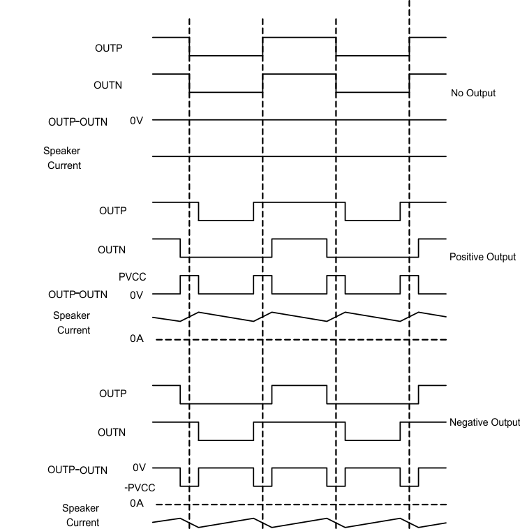
The TPA3136D2, TPA3136AD2 device is running in BD-modulation.
This is a modulation scheme that allows operation without the classic LC reconstruction filter when the amp is driving an inductive load with short speaker wires. Each output is switching from 0 volts to the supply voltage. The OUTPx and OUTNx are in phase with each other with no input so that there is little or no current in the speaker. The duty cycle of OUTPx is greater than 50% and OUTNx is less than 50% for positive output voltages. The duty cycle of OUTPx is less than 50% and OUTNx is greater than 50% for negative output voltages. The voltage across the load sits at 0 V throughout most of the switching period, reducing the switching current, which reduces any I2R losses in the load.
 Figure 17. BD Mode Modulation