SLOS956C June   2016  – January 2020 TPA3137D2

PRODUCTION DATA.  

  1. Features
  2. Applications
  3. Description
    1.     Device Images
      1.      Simplified Schematic
  4. Revision History
  5. Device Comparison Table
  6. Pin Configuration and Functions
    1.     Pin Functions
  7. Specifications
    1. 7.1 Absolute Maximum Ratings
    2. 7.2 ESD Ratings
    3. 7.3 Recommended Operating Conditions
    4. 7.4 Thermal Information
    5. 7.5 Electrical Characteristics
    6. 7.6 Switching Characteristics
    7. 7.7 Typical Characteristics
  8. Parameter Measurement Information
  9. Detailed Description
    1. 9.1 Overview
    2. 9.2 Functional Block Diagram
    3. 9.3 Feature Description
      1. 9.3.1 Fixed Analog Gain
      2. 9.3.2 SD Operation
      3. 9.3.3 PLIMIT
      4. 9.3.4 Spread Spectrum and De-Phase Control
      5. 9.3.5 GVDD Supply
      6. 9.3.6 DC Detect
      7. 9.3.7 PBTL Select
      8. 9.3.8 Short-Circuit Protection and Automatic Recovery Feature
      9. 9.3.9 Thermal Protection
    4. 9.4 Device Functional Modes
  10. 10Application and Implementation
    1. 10.1 Application Information
    2. 10.2 Typical Applications
      1. 10.2.1 Design Requirements
        1. 10.2.1.1 PCB Material Recommendation
        2. 10.2.1.2 PVCC Capacitor Recommendation
        3. 10.2.1.3 Decoupling Capacitor Recommendations
      2. 10.2.2 Detailed Design Procedure
        1. 10.2.2.1 Ferrite Bead Filter Considerations
        2. 10.2.2.2 Efficiency: LC Filter Required with the Traditional Class-D Modulation Scheme
        3. 10.2.2.3 When to Use an Output Filter for EMI Suppression
        4. 10.2.2.4 Input Resistance
        5. 10.2.2.5 Input Capacitor, Ci
        6. 10.2.2.6 BSN and BSP Capacitors
        7. 10.2.2.7 Differential Inputs
        8. 10.2.2.8 Using Low-ESR Capacitors
      3. 10.2.3 Application Performance Curves
        1. 10.2.3.1 EN55013 Radiated Emissions Results
        2. 10.2.3.2 EN55022 Conducted Emissions Results
  11. 11Power Supply Recommendations
    1. 11.1 Power Supply Decoupling, CS
  12. 12Layout
    1. 12.1 Layout Guidelines
    2. 12.2 Layout Example
  13. 13Device and Documentation Support
    1. 13.1 Device Support
      1. 13.1.1 Third-Party Products Disclaimer
    2. 13.2 Documentation Support
      1. 13.2.1 Related Documentation
    3. 13.3 Related Links
    4. 13.4 Receiving Notification of Documentation Updates
    5. 13.5 Support Resources
    6. 13.6 Trademarks
    7. 13.7 Electrostatic Discharge Caution
    8. 13.8 Glossary
  14. 14Mechanical, Packaging, and Orderable Information

パッケージ・オプション

メカニカル・データ(パッケージ|ピン)
サーマルパッド・メカニカル・データ
発注情報

Typical Characteristics

All Measurements taken at 26dB closed loop gain, 1-kHz audio, T A= 25°C unless otherwise noted. Measurements were made with AES17 filter using the TPA3137D2 EVM, which is available at ti.com.
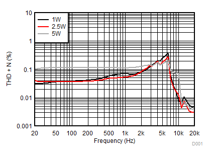
TPA3137D2 D001_SLOS938_TPA3136.gif
AVCC=PVCC = 12 V, Load = 6 Ω + 47 µH, 1 W, 2.5 W, 5 W
Figure 1. Total Harmonic Distortion vs Frequency (BTL)
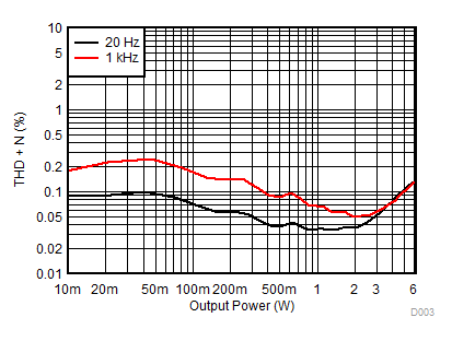
TPA3137D2 D003_SLOS956_TPA3137.gif
AVCC=PVCC = 12 V, Load = 6 Ω + 47 µH, 20 Hz, 1 kHz
Figure 3. Total Harmonic Distortion + Noise vs Output Power (BTL)
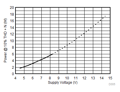
TPA3137D2 D005_SLOS956_TPA3137.gif
AVCC=PVCC = 4.5 V to 14.4 V, Load = 6 Ω + 47 µH
Figure 5. Output Power vs Supply Voltage (BTL)
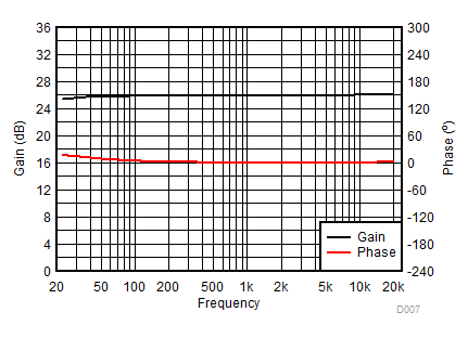
TPA3137D2 D007_SLOS938_TPA3136.gif
AVCC=PVCC = 12 V, Load = 6 Ω + 47 µH (device pins)
Figure 7. Gain/Phase vs Frequency (BTL)
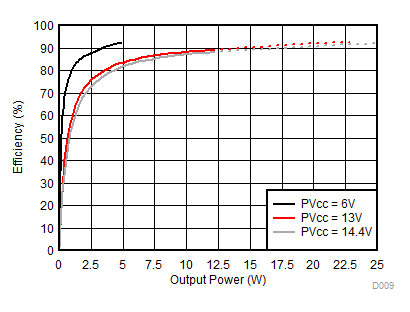
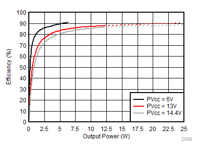
TPA3137D2 D009_SLOS956_TPA3137.gif
AVCC=PVCC= 6 V, 13 V, 14.4 V, Load = 8 Ω + 66 µH
Figure 9. Efficiency vs Output Power (BTL)
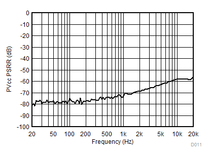
TPA3137D2 D011_SLOS938_TPA3136.gif
AVCC=PVCC = 12 V, Load = 4 Ω + 33 µH
Figure 11. Supply Ripple Rejection Ratio vs Frequency (BTL)
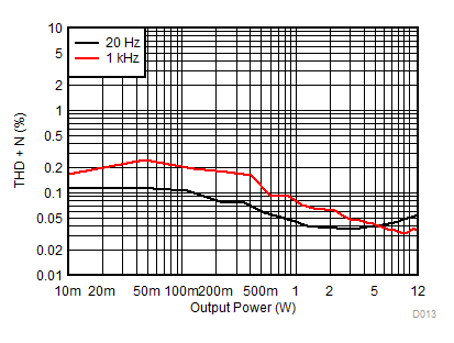
TPA3137D2 D013_SLOS956_TPA3137.gif
AVCC=PVCC = 13 V, Load = 4 Ω + 33 µH, 20 Hz, 1 kHz
Figure 13. Total Harmonic Distortion + Noise vs Output Power (PBTL)
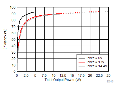
TPA3137D2 D015_SLOS956_TPA3137.gif
AVCC=PVCC = 6 V, 13 V, 14.4 V, Load = 4 Ω + 33 µH
Figure 15. Efficiency vs Output Power (PBTL)
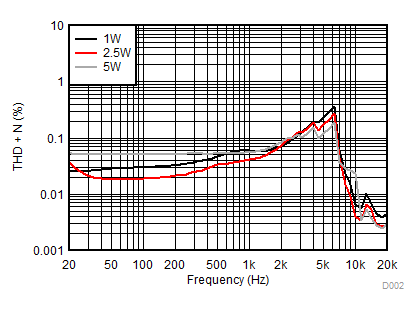
TPA3137D2 D002_SLOS938_TPA3136.gif
AVCC=PVCC = 13 V, Load = 8 Ω + 66 µH, 1 W, 2.5 W, 5 W
Figure 2. Total Harmonic Distortion vs Frequency (BTL)
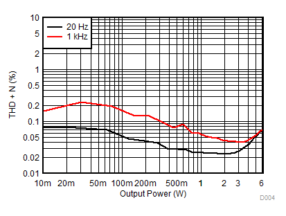
TPA3137D2 D004_SLOS956_TPA3137.gif
AVCC=PVCC = 13 V, Load = 8 Ω + 66 µH, 20 Hz, 1 kHz
Figure 4. Total Harmonic Distortion + Noise vs Output Power (BTL)
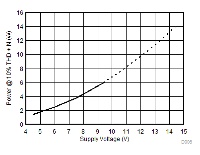
TPA3137D2 D006_SLOS956_TPA3137.gif
AVCC=PVCC = 4.5 V to 14.4 V, Load = 8 Ω + 66 µH
Figure 6. Output Power vs Supply Voltage (BTL)
TPA3137D2 D008_SLOS956_TPA3137.gif
AVCC=PVCC = 6 V, 12 V, 14.4 V, Load = 6 Ω + 47 µH
Figure 8. Efficiency vs Output Power (BTL)
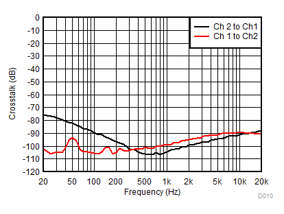
TPA3137D2 D010_SLOS938_TPA3136.gif
AVCC=PVCC = 12 V, 1 W, Load = 6 Ω + 47 µH
Figure 10. Crosstalk vs Frequency (BTL)
TPA3137D2 D012_SLOS938_TPA3136.gif
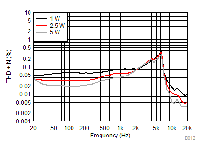
AVCC=PVCC = 13 V, Load = 4 Ω + 33 µH, 1 W, 2.5 W, 5 W
Figure 12. Total Harmonic Distortion + Noise vs Frequency (PBTL)
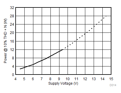
TPA3137D2 D014_SLOS956_TPA3137.gif
AVCC=PVCC = 4.5 V to 14.4 V, Load = 4 Ω + 33 µH
Figure 14. Output Power vs Supply Voltage (PBTL)