SLOS429C May 2004 – May 2016 TPA6204A1
PRODUCTION DATA.
- 1 Features
- 2 Applications
- 3 Description
- 4 Revision History
- 5 Device Comparison Table
- 6 Pin Configuration and Functions
- 7 Specifications
- 8 Parameter Measurement Information
- 9 Detailed Description
- 10Application and Implementation
- 11Power Supply Recommendations
- 12Layout
- 13Device and Documentation Support
- 14Mechanical, Packaging, and Orderable Information
パッケージ・オプション
デバイスごとのパッケージ図は、PDF版データシートをご参照ください。
メカニカル・データ(パッケージ|ピン)
- DRB|8
サーマルパッド・メカニカル・データ
- DRB|8
発注情報
10 Application and Implementation
NOTE
Information in the following applications sections is not part of the TI component specification, and TI does not warrant its accuracy or completeness. TI’s customers are responsible for determining suitability of components for their purposes. Customers should validate and test their design implementation to confirm system functionality.
10.1 Application Information
The TPA6204A1 device starts its operation by asserting the SHUTDOWN pin to logic 1. The device enters in shutdown mode when pulling the SHUTDOWN pin low. This typical connection diagram highlights the required external components and system level connections for proper operation of the device in popular use case. Any design variation can be supported by TI through schematic and layout reviews. Visit e2e.ti.com for design assistance and join the audio amplifier discussion forum for additional information.
10.2 Typical Application
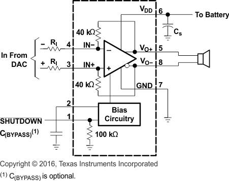
Figure 16 shows a typical circuit for the TPA6204A1 with a speaker, input resistors and supporting power supply capacitors.
 Figure 16. Typical Differential Input Application Schematic
10.2.1 Design Requirements
Table 4 lists the design parameters for this example.
Table 4. Design Parameters
| PARAMETER | EXAMPLE VALUE | |||
|---|---|---|---|---|
| Power supply | 2.5 V to 5 V | |||
| Current | 1 A | |||
| Speaker | 8 Ω | |||
10.2.2 Detailed Design Procedure
10.2.2.1 Selecting Components for Resistors (RI)
The input resistor (RI) can be selected to set the gain of the amplifier according to Equation 8.
The internal feedback resistors (RF) are trimmed to 40 kΩ. Resistor matching is very important in fully differential amplifiers. The balance of the output on the reference voltage depends on matched ratios of the resistors. CMRR, PSRR, and the cancellation of the second harmonic distortion diminishes if resistor mismatch occurs. Therefore, TI recommends using 1% tolerance resistors or better to keep the performance optimized.
10.2.2.2 Using Low-ESR Capacitors
Low-ESR capacitors are recommended throughout this applications section. A real (as opposed to ideal) capacitor can be modeled simply as a resistor in series with an ideal capacitor. The voltage drop across this resistor minimizes the beneficial effects of the capacitor in the circuit. The lower the equivalent value of this resistance the more the real capacitor behaves like an ideal capacitor.
10.2.2.2.1 Bypass Capacitor (C(BYPASS)) and Start-Up Time
The internal voltage divider at the BYPASS pin of this device sets a mid-supply voltage for internal references and sets the output common-mode voltage to VDD/2. Adding a capacitor to this pin filters any noise into this pin and increases kSVR. C(BYPASS) also determines the rise time of VO+ and VO− when the device is taken out of shutdown. The larger the capacitor, the slower the rise time. Figure 10 shows the relationship of C(BYPASS) to start-up time.
10.2.2.2.2 Input Capacitor (CI)
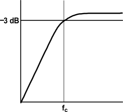
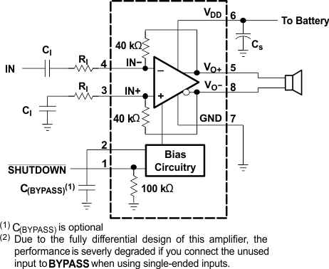
The TPA6204A1 does not require input coupling capacitors if using a differential input source that is biased from 0.5 V to VDD − 0.8 V. Use 1% tolerance or better gain-setting resistors if not using input coupling capacitors. In the single-ended input application an input capacitor, CI, is required to allow the amplifier to bias the input signal to the proper DC level. In this case, CI and RI form a high-pass filter with the corner frequency determined in Equation 9.

 Figure 17. CI and RI High-Pass Filter Cutoff Frequency
The value of CI is important to consider as it directly affects the bass (low frequency) performance of the circuit. Consider the example where RI is 10 kΩ and the specification calls for a flat bass response down to 100 Hz. Equation 9 is reconfigured as Equation 10.

In this example, CI is 0.16 μF, so one would likely choose a value in the range of 0.22 μF to 0.47 μF. Ceramic capacitors should be used when possible, as they are the best choice in preventing leakage current. When polarized capacitors are used, the positive side of the capacitor must face the amplifier input in most applications, as the DC level there is held at VDD/2, which is likely higher than the source DC level. It is important to confirm the capacitor polarity in the application.
10.2.2.2.3 Decoupling Capacitor (CS)
The TPA6204A1 is a high-performance CMOS audio amplifier that requires adequate power supply decoupling to ensure the output total harmonic distortion (THD) is as low as possible. Power supply decoupling also prevents oscillations for long lead lengths between the amplifier and the speaker. For higher frequency transients, spikes, or digital hash on the line, a good low equivalent-series resistance (ESR) ceramic capacitor, typically 0.1 μF to
1 μF, placed as close as possible to the device VDD lead works best. For filtering lower frequency noise signals, a 10-μF or greater capacitor placed near the audio power amplifier also helps, but is not required in most applications because of the high PSRR of this device.
10.2.3 Application Curves
For application curves, see the figures listed in Table 5.
Table 5. Table of Graphs
| FIGURE | |||
|---|---|---|---|
| PO | Output power | vs Supply voltage | Figure 1 |
| vs Load resistance | Figure 2 | ||
| PD | Power dissipation | vs Output power | Figure 3 |
| THD+N | Total harmonic distortion + noise | vs Output power | Figure 4 |
| vs Frequency | Figure 5 | ||
| vs Common-mode input voltage | Figure 6 | ||
| KSVR | Supply voltage rejection ratio | vs Frequency | Figure 7 |
| GSM Power supply rejection | vs Time | Figure 8 | |
| GSM Power supply rejection | vs Frequency | Figure 9 | |
| Closed-loop gain/phase | vs Frequency | Figure 10 | |
10.3 System Examples
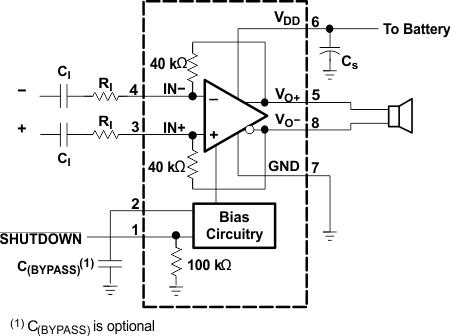
Figure 18 through Figure 19 show application schematics for differential and single-ended inputs. Typical values are shown in Table 6.
Table 6. Typical Component Values
| COMPONENT | VALUE |
|---|---|
| RI | 40 kΩ |
| C(BYPASS) | 0.22 µF |
| CS | 1 µF |
| CI | 0.22 µF |
 Figure 18. Differential Input Application Schematic Optimized With Input Capacitors
