SLVSDG9B March 2016 – December 2016 TPD1E0B04
PRODUCTION DATA.
- 1 Features
- 2 Applications
- 3 Description
- 4 Revision History
- 5 Pin Configuration and Functions
- 6 Specifications
-
7 Detailed Description
- 7.1 Overview
- 7.2 Functional Block Diagram
- 7.3
Feature Description
- 7.3.1 IEC 61000-4-2 ESD Protection
- 7.3.2 IEC 61000-4-4 EFT Protection
- 7.3.3 IEC 61000-4-5 Surge Protection
- 7.3.4 IO Capacitance
- 7.3.5 DC Breakdown Voltage
- 7.3.6 Ultra Low Leakage Current
- 7.3.7 Low ESD Clamping Voltage
- 7.3.8 Supports High Speed Interfaces
- 7.3.9 Industrial Temperature Range
- 7.3.10 Industry Standard Package
- 7.4 Device Functional Modes
- 8 Application and Implementation
- 9 Power Supply Recommendations
- 10Layout
- 11Device and Documentation Support
- 12Mechanical, Packaging, and Orderable Information
パッケージ・オプション
メカニカル・データ(パッケージ|ピン)
サーマルパッド・メカニカル・データ
発注情報
6 Specifications
6.1 Absolute Maximum Ratings
over operating free-air temperature range (unless otherwise noted)(1)| MIN | MAX | UNIT | ||
|---|---|---|---|---|
| Electrical fast transient | IEC 61000-4-5 (5/50 ns) | 80 | A | |
| Peak pulse | IEC 61000-4-5 power (tp - 8/20 µs) | 15 | W | |
| IEC 61000-4-5 current (tp - 8/20 µs) | 1.7 | A | ||
| TA | Operating free-air temperature | –40 | 125 | °C |
| Tstg | Storage temperature | –65 | 155 | °C |
(1) Stresses beyond those listed under Absolute Maximum Ratings may cause permanent damage to the device. These are stress ratings only, which do not imply functional operation of the device at these or any other conditions beyond those indicated under Recommended Operating Conditions. Exposure to absolute-maximum-rated conditions for extended periods may affect device reliability.
6.2 ESD Ratings
| VALUE | UNIT | |||
|---|---|---|---|---|
| V(ESD) | Electrostatic discharge | Human-body model (HBM), per ANSI/ESDA/JEDEC JS-001(1) | ±2500 | V |
| Charged-device model (CDM), per JEDEC specification JESD22-C101(2) | ±1000 | |||
(1) JEDEC document JEP155 states that 500-V HBM allows safe manufacturing with a standard ESD control process.
(2) JEDEC document JEP157 states that 250-V CDM allows safe manufacturing with a standard ESD control process.
6.3 ESD Ratings—IEC Specification
| VALUE | UNIT | |||
|---|---|---|---|---|
| V(ESD) | Electrostatic discharge | IEC 61000-4-2 contact discharge | ±8000 | V |
| IEC 61000-4-2 air-gap discharge | ±9000 | |||
6.4 Recommended Operating Conditions
over operating free-air temperature range (unless otherwise noted)| MIN | MAX | UNIT | ||
|---|---|---|---|---|
| VIO | Input pin voltage | –3.6 | 3.6 | V |
| TA | Operating free-air temperature | –40 | 125 | °C |
6.5 Thermal Information
| THERMAL METRIC(1) | TPD1E0B04 | UNIT | ||
|---|---|---|---|---|
| DPL (X2SON) | DPY (X1SON) | |||
| 2 PINS | 2 PINS | |||
| RθJA | Junction-to-ambient thermal resistance | 582 | 442.6 | °C/W |
| RθJC(top) | Junction-to-case (top) thermal resistance | 264.5 | 243.8 | °C/W |
| RθJB | Junction-to-board thermal resistance | 394.4 | 162.5 | °C/W |
| ψJT | Junction-to-top characterization parameter | 36.4 | 154.1 | °C/W |
| ψJB | Junction-to-board characterization parameter | 394.4 | 163.0 | °C/W |
| RθJC(bot) | Junction-to-case (bottom) thermal resistance | n/a | n/a | °C/W |
(1) For more information about traditional and new thermal metrics, see the Semiconductor and IC Package Thermal Metrics application report.
6.6 Electrical Characteristics
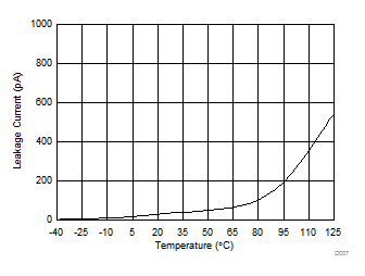
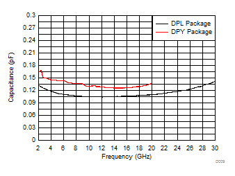
over operating free-air temperature range (unless otherwise noted)6.7 Typical Characteristics
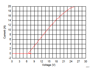
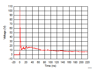
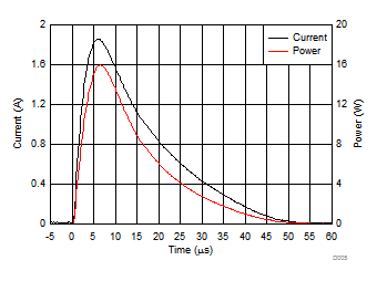
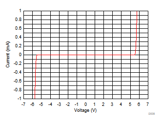
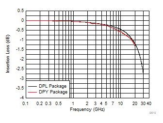
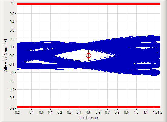
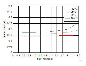
(Bare Board)
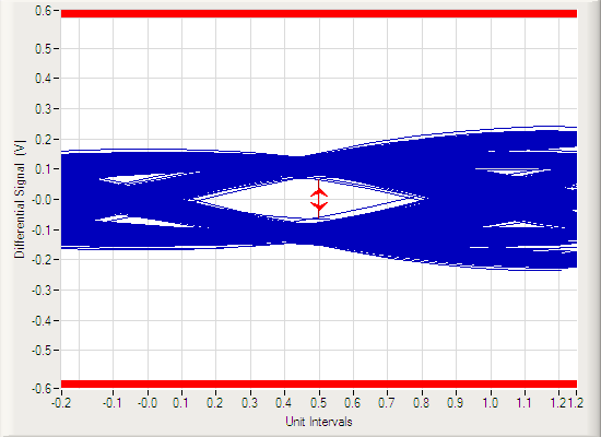
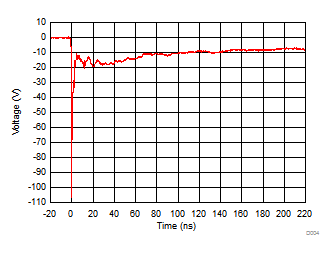
(with TPD1E0B04DPL)
