SLVS953B June 2009 – August 2015 TPD2E009
PRODUCTION DATA.
- 1 Features
- 2 Applications
- 3 Description
- 4 Revision History
- 5 Pin Configuration and Functions
- 6 Specifications
- 7 Detailed Description
- 8 Application and Implementation
- 9 Power Supply Recommendations
- 10Layout
- 11Device and Documentation Support
- 12Mechanical, Packaging, and Orderable Information
パッケージ・オプション
メカニカル・データ(パッケージ|ピン)
サーマルパッド・メカニカル・データ
- DRT|3
発注情報
6 Specifications
6.1 Absolute Maximum Ratings(1)
over operating free-air temperature range (unless otherwise noted)| MIN | MAX | UNIT | |||
|---|---|---|---|---|---|
| Operating temperature | –40 | 85 | °C | ||
| I/O voltage tolerance | D+, D– pins | 0 | 6 | V | |
| Peak pulse current (tp = 8/20 μs) | 5 | A | |||
| Peak pulse power (tp = 8/20 μs) | 45 | W | |||
| Storage temperature, Tstg | –65 | 125 | °C | ||
(1) Stresses beyond those listed under Absolute Maximum Ratings may cause permanent damage to the device. These are stress ratings only, and functional operation of the device at these or any other conditions beyond those indicated in the operational sections of the specifications is not implied. Exposure to absolute maximum-rated conditions for extended periods may affect device reliability.
6.2 ESD Ratings
| VALUE | UNIT | ||||
|---|---|---|---|---|---|
| V(ESD) | Electrostatic discharge | Human body model (HBM), per ANSI/ESDA/JEDEC JS-001(1) | ±15000 | V | |
| Charged-device model (CDM), per JEDEC specification JESD22-C101(2) | ±1000 | ||||
| IEC 61000-4-2 contact discharge | D+, D– pins | ±8000 | |||
| IEC 61000-4-2 air-gap discharge | D+, D– pins | ±8000 | |||
(1) JEDEC document JEP155 states that 500-V HBM allows safe manufacturing with a standard ESD control process.
(2) JEDEC document JEP157 states that 250-V CDM allows safe manufacturing with a standard ESD control process.
6.3 Recommended Operating Conditions
over operating free-air temperature range (unless otherwise noted)| MIN | NOM | MAX | UNIT | ||
|---|---|---|---|---|---|
| Operating free-air temperature, TA | –40 | 85 | °C | ||
| Operating voltage | Pin 1 or 2 to 3 or Pin 3 to 1 or 2 | 0 | 5.5 | V | |
6.4 Thermal Information
| THERMAL METRIC(1) | TPD2E009 | UNIT | ||
|---|---|---|---|---|
| DBZ (SOT) | DRT (SOT) | |||
| 3 PINS | 3 PINS | |||
| RθJA | Junction-to-ambient thermal resistance | 461.8 | 610 | °C/W |
| RθJC(top) | Junction-to-case (top) thermal resistance | 216.2 | 288 | °C/W |
| RθJB | Junction-to-board thermal resistance | 195.6 | 118.4 | °C/W |
| ψJT | Junction-to-top characterization parameter | 70.1 | 20.2 | °C/W |
| ψJB | Junction-to-board characterization parameter | 193.7 | 116.4 | °C/W |
(1) For more information about traditional and new thermal metrics, see the Semiconductor and IC Package Thermal Metrics application report, SPRA953.
6.5 Electrical Characteristics
over operating free-air temperature range (unless otherwise noted)| PARAMETER | TEST CONDITIONS | MIN | TYP | MAX | UNIT | ||
|---|---|---|---|---|---|---|---|
| VRWM | Reverse stand-off voltage | D+, D– pins to ground | 5.5 | V | |||
| VCLAMP | Clamp voltage | D+, D– pins to ground, | IIO = 1 A | 8 | V | ||
| IIO | Current from I/O port to supply pins | VIO = 2.5 V | 0.01 | 0.1 | μA | ||
| VD | Diode forward voltage | D+, D– pins, lower clamp diode, |
VIO = 2.5 V, ID = 8 mA | 0.6 | 0.8 | 0.95 | V |
| D+, D– pins, upper clamp diode, DRY package |
VCC = 0 V, ID = –8 mA | 0.6 | 0.8 | 0.95 | |||
| RDYN | Dynamic resistance | D+, D– pins, | I = 1 A | 1 | Ω | ||
| CIO | I/O capacitance | D+, D– pins, DBZ Package | VIO = 2.5 V, f = 10 MHz | 0.9 | pF | ||
| D+, D– pins, DRT Package | VIO = 2.5 V, f = 10 MHz | 0.7 | pF | ||||
| VBR | Break-down voltage | IIO = 1 mA | 7 | V | |||
6.6 Typical Characteristics
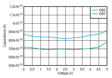 Figure 1. I/O Capacitance vs I/O Voltage (TA= 25°C)
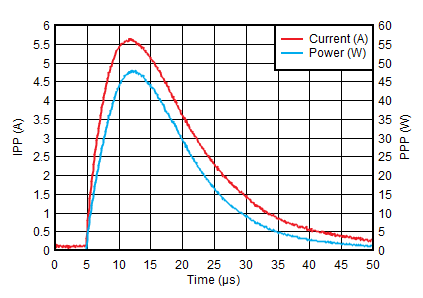
(Measured at One I/O, With the Other I/O Open)
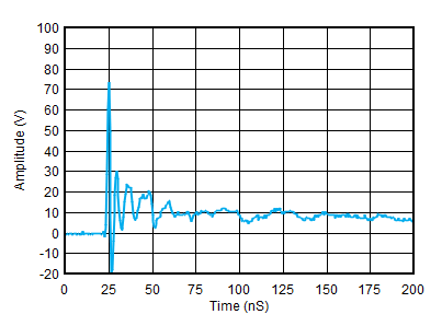 Figure 5. IEC Clamping Waveforms (8-kV Contact)
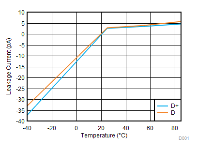 Figure 2. Leakage Current vs Temperature (VIO = 2.5 V)
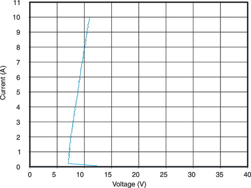 Figure 4. D+, D– Transmission Line Pulser Plot
 (100-ns Pulse, 10-ns Rise Time)
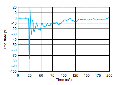 Figure 6. IEC Clamping Waveforms (–8-kV Contact)