JAJSJ53B may 2020 – april 2023 TPD3S713-Q1 , TPD3S713A-Q1
PRODUCTION DATA
- 1
- 1 特長
- 2 アプリケーション
- 3 概要
- 4 Revision History
- 5 Pin Configuration and Functions
- 6 Specifications
- 7 Parameter Measurement Information
- 8 Detailed Description
- 9 Application and Implementation
- 10Device and Documentation Support
- 11Mechanical, Packaging, and Orderable Information
パッケージ・オプション
デバイスごとのパッケージ図は、PDF版データシートをご参照ください。
メカニカル・データ(パッケージ|ピン)
- RVC|20
サーマルパッド・メカニカル・データ
- RVC|20
発注情報
8.3.9 Current-Limit Setting
The TPD3S713x-Q1 has two independent current-limit settings that are each adjusted externally with a resistor. The ILIM_HI setting is adjusted with R(ILIM_HI) connected between ILIM_HI and GND. The ILIM_LO setting is adjusted with R(ILIM_LO) connected between ILIM_LO and GND.
The current limit is selected by ILIM_SEL pin. If ILIM_SEL = high, ILIM_HI is selected; if ILIM_SEL = low, ILIM_LO is selected.
The following equation calculates the value of resistor for adjusting the typical current limit (need update):
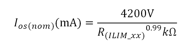
Many applications require that the current limit meet specific tolerance limits. When designing to these tolerance limits, both the tolerance of the TPD3S713x-Q1 current limit and the tolerance of the external adjusting resistor must be taken into account. The following equations approximate the TPD3S713x-Q1 minimum and maximum current limits to within a few milliamperes and are appropriate for design purposes. The equations do not constitute part of TI’s published device specifications for purposes of TI’s product warranty. These equations assume an ideal—no variation—external adjusting resistor. To take resistor tolerance into account, first determine the minimum and maximum resistor values based on its tolerance specifications and use these values in the equations. Because of the inverse relation between the current limit and the adjusting resistor, use the maximum resistor value in the IOS(min) equation and the minimum resistor value in the IOS(max) equation.
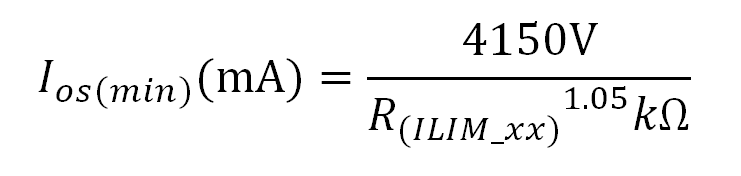
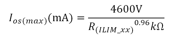
 Figure 8-3 Current-Limit Setting vs Adjusting Resistor
The routing of the traces to the R(ILIM_xx) resistors must have a sufficiently low resistance so as not to affect the current-limit accuracy. The ground connection for the R(ILIM_xx) resistors is also very important. The resistors must reference back to the TPD3S713x-Q1 GND pin. Follow normal board layout practices to ensure that current flow from other parts of the board does not impact the ground potential between the resistors and the TPD3S713x-Q1 GND pin.